The story behind this project
Every now and then I would find the need for a differential probe. I’d end up using a high voltage diff probe, which you've probably seen lurking around most electronics labs – the ones housed in a large rectangular box with a pair of heavy leads dangling out one end. While great for high voltage work, they were a hassle for general purpose measurements. Those giant leads are not a good match for probing small components. Their high attenuation levels resulted in noisy measurements at lower voltages. I was always left wondering if I could trust higher frequency measurements, with the leads dangling between the probe and device under test and flopping onto the PCB.
That got me thinking . . . is there a decent smaller probe out there to add to my lab? Could you use something like it too? It turns out that the big name test equipment companies have some really nice diff probes, many exceeding 100MHz bandwidth. However, the prices start in the thousands, and often have a brand-specific interface.
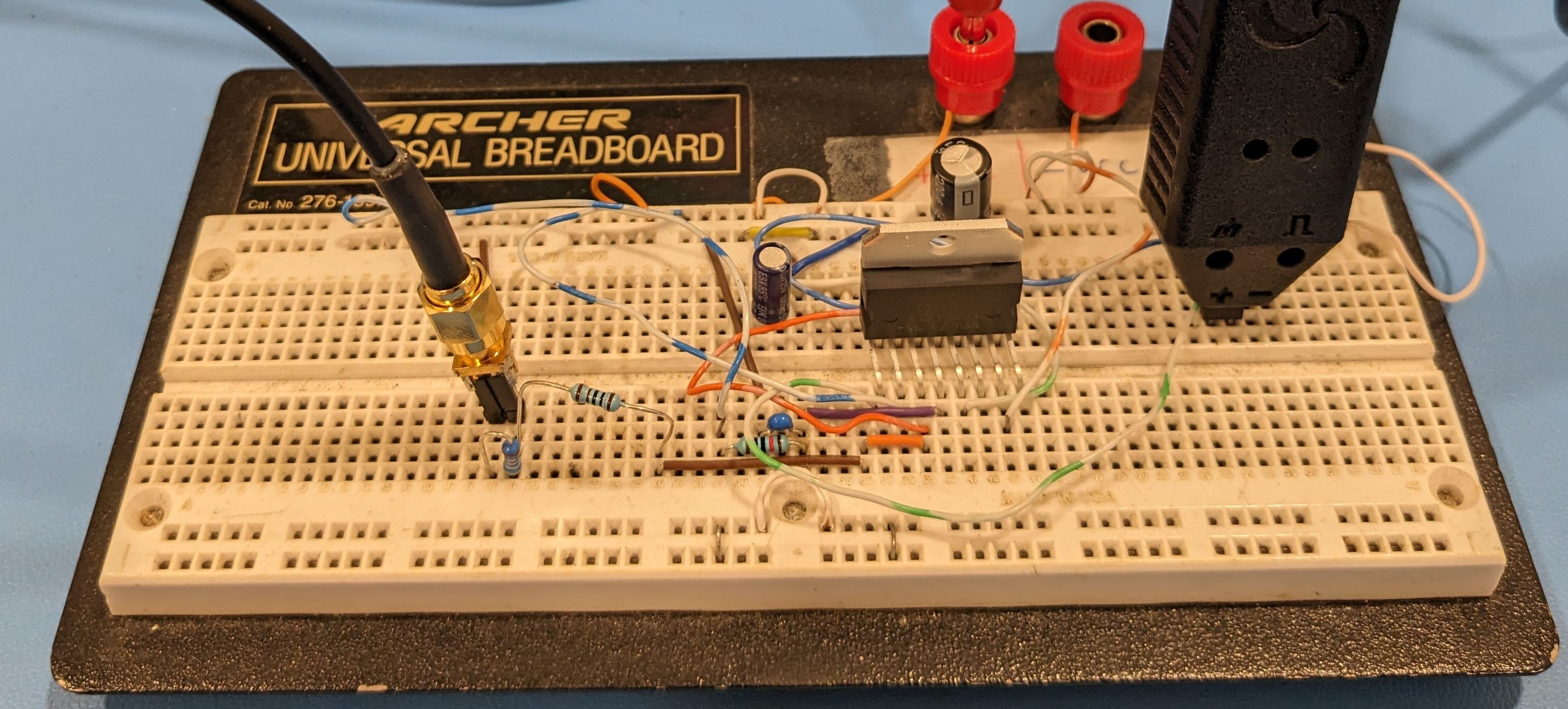
So, I figured, it can’t be that hard to build one and started reading up on how they work. Armed with modest goals and a little knowledge, I went about designing a simple 10 MHz-ish probe. It seemed very doable . . . but then I thought, 100MHz bandwidth would be nice, or maybe a little more. Things got harder, but maybe still doable. It would also be nice to get rid of the potentiometers and other annoying adjustments that you need to get good common mode rejection and DC offset and so on. Oh, and it would be nice to have an insulated enclosure. Now the design was getting tricky and I got bogged down. A little more scope creep later, this project was born!
HACKADAY project goals
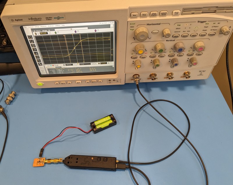
Many months and iterations later led to what you see in the project photos. It suits my diff probe needs for now, so what next? I figured I would get the design out there, so you could build it if you’d like. Or if there’s enough interest, iron out some of its rough edges and make a product of it. I’m happy to hear your feedback, so feel free to comment.
Specs & features at glance
Okay, so that’s all well and good, but what can this thing do? I did my best to balance cost and complexity and came up with the following specs and features. So without further ado, here they are:
Specs:
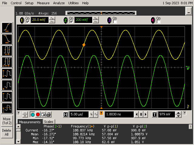
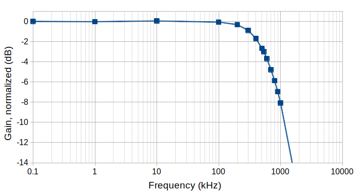
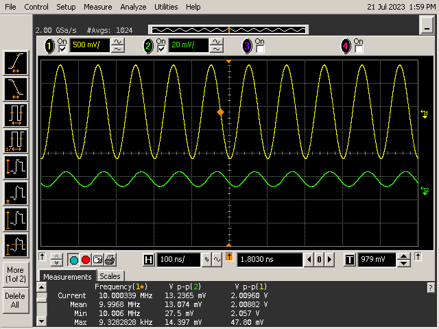
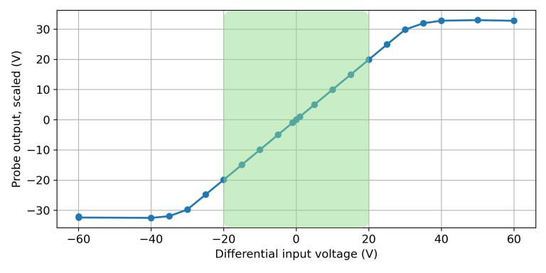
| Bandwidth, 3 dB | ≥150 MHz |
| Attenuation | 20:1 |
| Differential signal range | ±20 V |
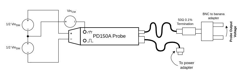
| Common mode range | ±30 V |
| DC offset voltage | ≤ ± 10 mV, referenced to input, after zeroing |
| CMRR, 60 Hz | ≥ 70 dB, referenced to input |
| CMRR, 10 MHz | ≥ 40 dB, referenced to input |
| Input Resistance, between inputs | 1.08 MΩ between inputs, 540 kΩ from each input to ground |
| Input Capacitance at 10 kHz | ≤ 3 pF between inputs, ≤ 6 pF from each input to ground, typical |
| DC Attenuation Accuracy | ≤ ± 5% |
| Pulse Rise Time (10% to 90%) | ≤ 2.4 ns |
| Gain Flatness, 0-30 MHz | ≤ ± 0.5 dB , typical |
| Input Damage Threshold | 100 V |
Features:
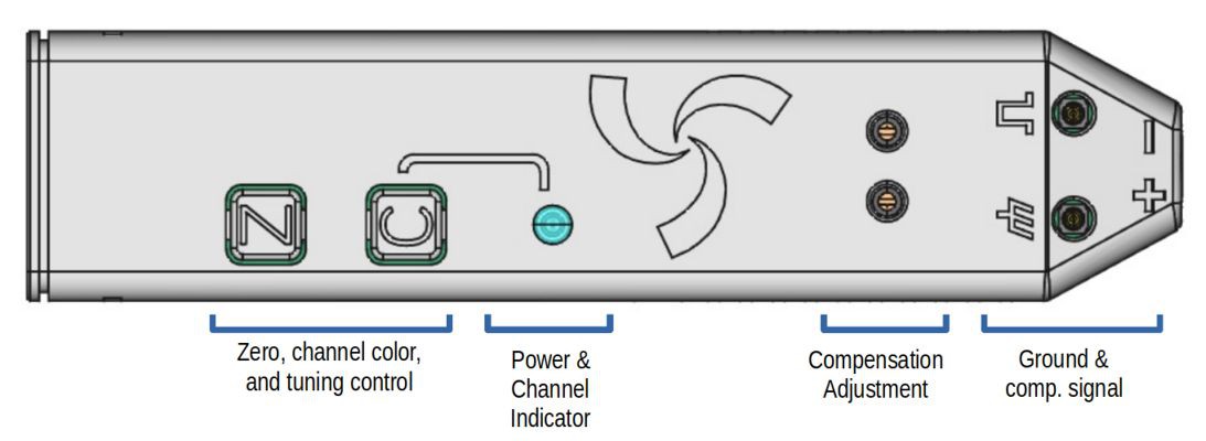
LED scope channel indicator: This helps you keep track of what scope channel the probe is connected to, especially if you're
using more than one diff probe for a test. PD150's LED color can be set
to any standard scope channel color. Use the "C" button to cycle
through colors.
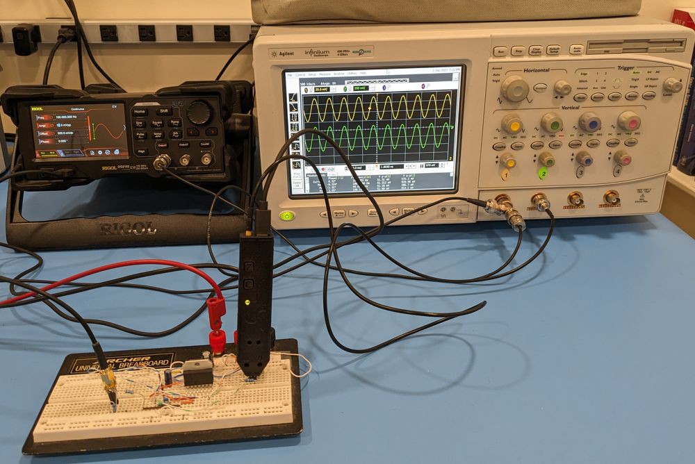
- Flexible probe interface: The probe inputs are simply 0.1-inch spaced sockets. Their close spacing is good for measuring higher frequency or sensitive signals. You can solder a header to the circuit to connect to. For less critical work, you can attach jumper wires.
- USB Power: PD150 is powered through a USB-C connector. It needs 5V at 300 mA, which can be provided by a small adapter or many USB ports.
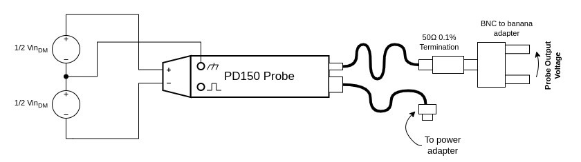
- Scope compatibility: PD150 has a BNC signal cable and 50 Ω output impedance. Thus you can connect it directly to a scope with a 50 Ω input, so long as its rated for at least 2.5 Vrms. For scopes with only a high impedance input, you can use a 50 Ω inline attenuator...


 Vedran
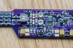
 Bud Bennett
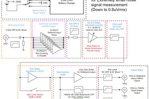
 Floydfish
Really nice! How much noise to you get on the output signal?