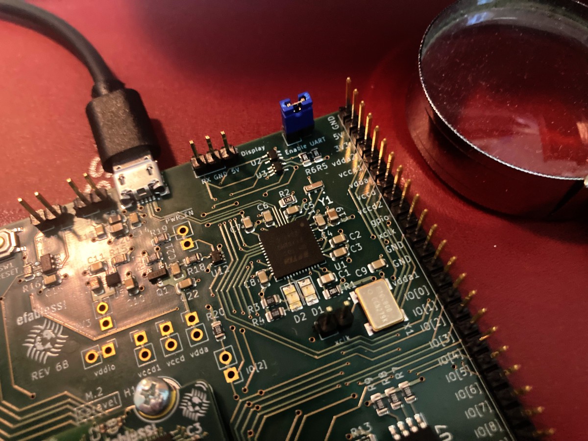
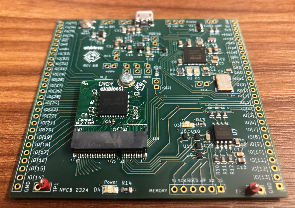
Close
0%
0%

Lab Computer "Marina"

How many Caravel chips does it take to make a usable lab computer for debugging digital electronics? Let's find out...

Public Chat
Similar projects worth following
So I plan to build lab computer "Marina" out of efabless' Caravel chips. "Caravel" is a RISC-V microcontroller embedded in every OpenMPW or chipIgnite custom logic chip from efabless (I will use 5V chips from recent GFMPW0 shuttle). It's fully open-sourced VexRiscv-based (in relatively recent designs) RV32I core with onboard 2KB SRAM and ability to run code directly from SPI-flash (with 16-instruction cache it's having kind of acceptable performance) and from onboard SRAM (much faster, but through the same 16-instruction cache). Also it has access to about 30 user IOs that could be re-programmed to be connected to user logic design inside the chip or to outside pins making Caravel perfect MCU to debug 5V electronics...

Efabless daughter-board with Caravel chip uses edge connector that is called "M.2 Keyed E" (it's SparkFun's MicroMod form-factor, but with totally different pinout):

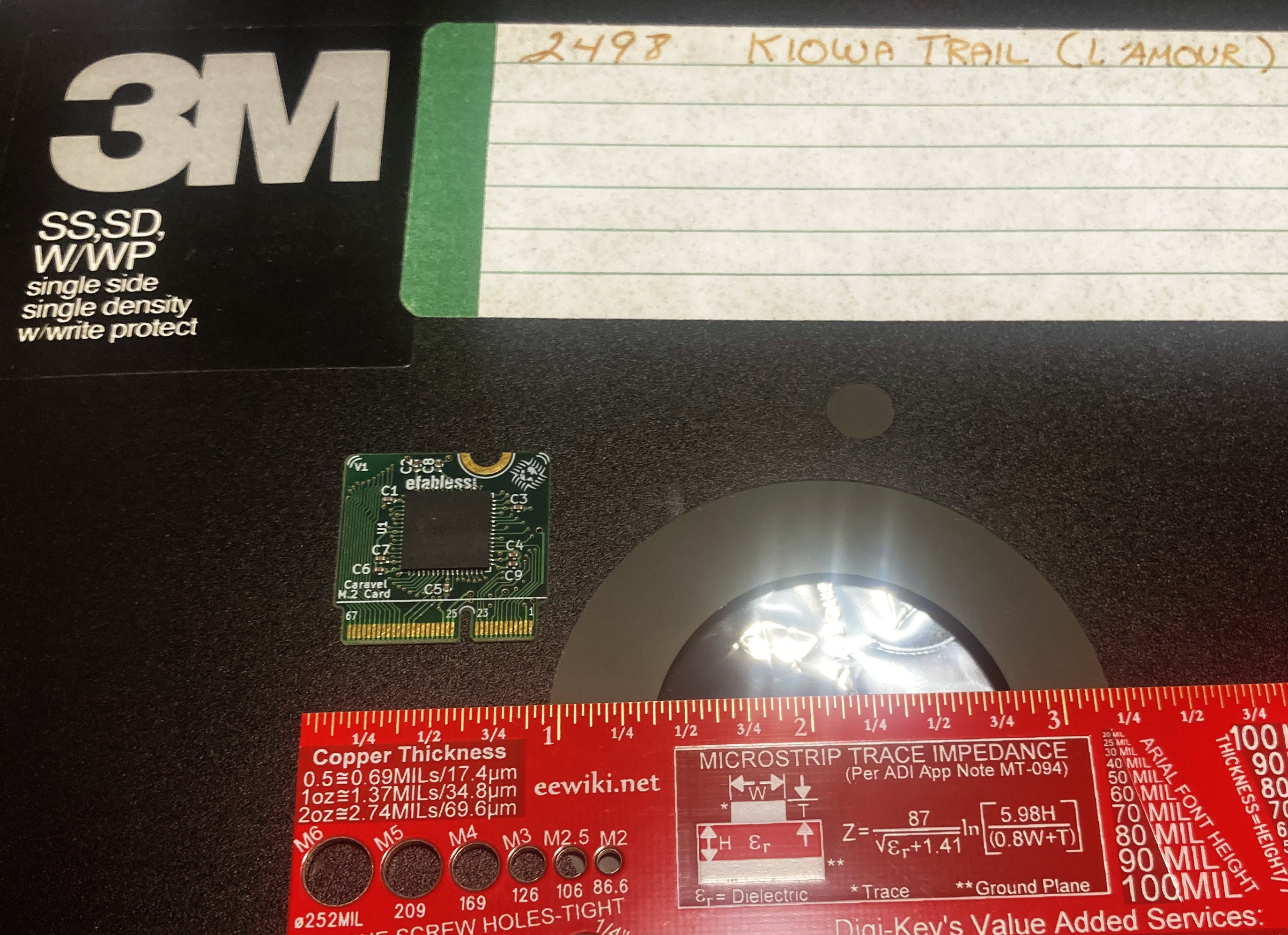
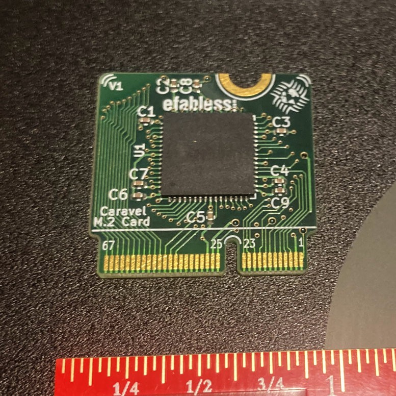
To play with it those chips (I have a few) I decided to make a breakout board with proper connector pre-soldered by PCB manufacturer:

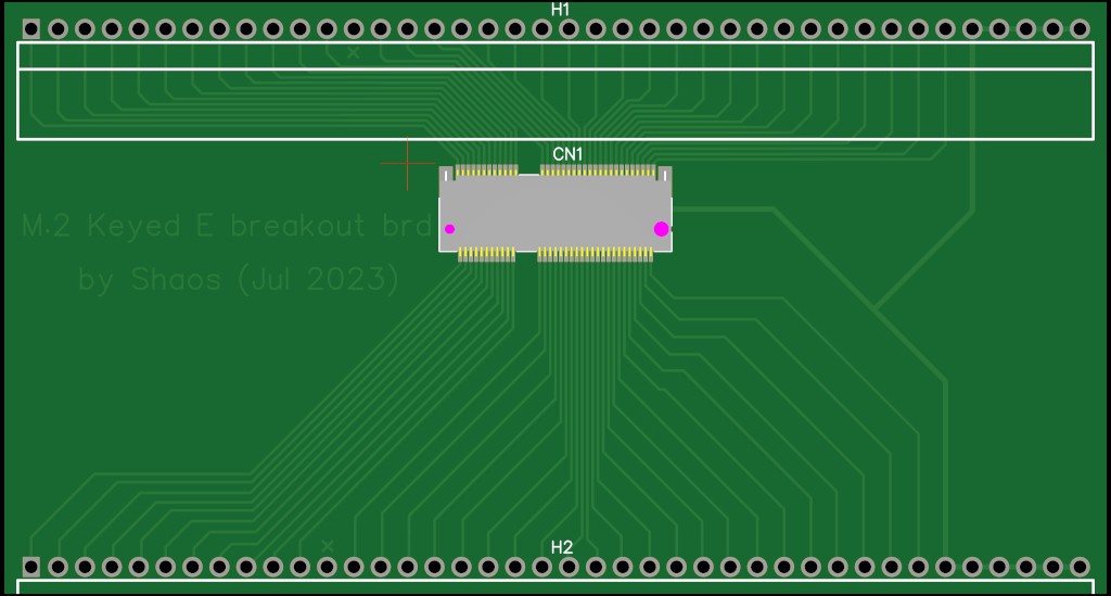
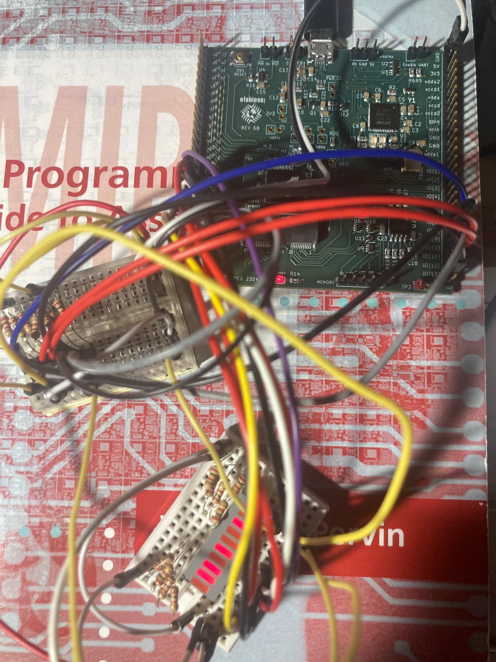
Plan is to use one or more Caravel chips to build a usable computer (codename "Marina") that may help to debug 5V digital electronics (including retrocomputers and old microprocessors). I expect a lot of fun here :)

M.2.breakout.ods

Pinout of the M.2 breakout board with Caravel chip

spreadsheet - 17.02 kB - 07/26/2023 at 06:13

Download

M.2.breakout-Schematics.png

M.2 breakout board schematics

Portable Network Graphics (PNG) - 156.18 kB - 07/26/2023 at 06:12

Preview
Download

M.2.breakout-BOM-Placement.zip

BOM and Peak&Place files for M.2 breakout board

Zip Archive - 775.00 bytes - 07/26/2023 at 06:11

Download

Gerber_NEW_PCB_2023-07-20.zip

Gerber-files for M.2 breakout board production

Zip Archive - 10.48 kB - 07/26/2023 at 06:10

Download

  • How to test custom logic part of Caravel chip

    SHAOS08/17/2023 at 06:40 1 comment

    I moved everything needed to my own repo: https://gitlab.com/shaos/marina

    For example this is my own location of original blink program:

    https://gitlab.com/shaos/marina/-/blob/main/blink/blink.c

    If you look into function void configure_io() you may see how IOs are configured:

    • from reg_mprj_io_0 to reg_mprj_io_6 (somebody said up to reg_mprj_io_7) are occupied by the system;
    • then up to reg_mprj_io_35 could be used by user (and may be even reg_mprj_io_36 and reg_mprj_io_37 - so it's like 30 IOs).
      //  ======= set each IO to the desired configuration =============
      
          //  GPIO 0 is turned off to prevent toggling the debug pin; For debug, make this an output and
          //  drive it externally to ground.
      
          reg_mprj_io_0 = GPIO_MODE_MGMT_STD_INPUT_NOPULL;
      
          // Changing configuration for IO[1-4] will interfere with programming flash. if you change them,
          // You may need to hold reset while powering up the board and initiating flash to keep the process
          // configuring these IO from their default values.
      
          reg_mprj_io_1 = GPIO_MODE_MGMT_STD_OUTPUT;
          reg_mprj_io_2 = GPIO_MODE_MGMT_STD_INPUT_NOPULL;
          reg_mprj_io_3 = GPIO_MODE_MGMT_STD_INPUT_NOPULL;
          reg_mprj_io_4 = GPIO_MODE_MGMT_STD_INPUT_NOPULL;
      
          // -------------------------------------------
      
          reg_mprj_io_5 = GPIO_MODE_MGMT_STD_INPUT_NOPULL;     // UART Rx
          reg_mprj_io_6 = GPIO_MODE_MGMT_STD_OUTPUT;           // UART Tx
          reg_mprj_io_7 = GPIO_MODE_MGMT_STD_OUTPUT;
      
          ...
      
          reg_mprj_io_37 = GPIO_MODE_MGMT_STD_OUTPUT;
      
          // Initiate the serial transfer to configure IO
          reg_mprj_xfer = 1;
          while (reg_mprj_xfer == 1);

    At the end of the function you can see how it sets those configuration values to the actual hardware. Before calling this function it's also setting up the only GPIO pin (that is connected to LED in efabless "mother" board):

        reg_gpio_mode1 = 1;
        reg_gpio_mode0 = 0;
        reg_gpio_ien = 1;
        reg_gpio_oeb = 0;
    

    It's basically means OUTPUT and it must be OUTPUT (inverted indication):

    Then to switch LED On we need to write there 0 and to switch LED Off we need to write there 1:

    	while (1) {
    
            reg_gpio_out = 1; // OFF
            reg_mprj_datah = 0x0000002a;
            reg_mprj_datal = 0xaaaaaaaa;
    
    //		delay(50000);
    		delay(2000000);
    
            reg_gpio_out = 0;  // ON
            reg_mprj_datah = 0x00000015;
            reg_mprj_datal = 0x55555555;
    
    //		delay(50000);
    		delay(2000000);
    
        }
    

    Here also clearly visible way to program IOs - reg_mprj_datal covers lower 32 bits, and reg_mprj_datah cover higher 6 bits (if it's defined as inputs you can read from those variables as well).

    In this case on-board custom logic is not connected to anything - everything is controlled by RISC-V programmatically, but what if we need to connect IOs to user custom logic? Then IOs must be configured to one of this settings:

    //      GPIO_MODE_USER_STD_INPUT_NOPULL
    //      GPIO_MODE_USER_STD_INPUT_PULLDOWN
    //      GPIO_MODE_USER_STD_INPUT_PULLUP
    //      GPIO_MODE_USER_STD_OUTPUT
    //      GPIO_MODE_USER_STD_BIDIRECTIONAL
    //      GPIO_MODE_USER_STD_ANALOG
    

    But then Caravel RISC-V will not be able to read or write IOs, so what can be done to programmatically write user inputs and read user outputs? TinyTapeout discord user anish experimentally found bits that need to be set for this:

    #define GPIO_MODE_MGMT_CONTROLLED_IO 0x00F
    #define GPIO_MODE_USER_CONTROLLED_IO 0x00E
    

    So we set user custom design inputs to GPIO_MODE_MGMT_CONTROLLED_IO and user custom design outputs to GPIO_MODE_USER_CONTROLLED_IO (Note: I gave those macro names. Names proposed by anish were different). Now we can build custom tester of on-board custom logic:

    https://gitlab.com/shaos/marina/-/blob/main/shaos_test1/main.c?ref_type=heads

  • Start with Caravel

    SHAOS07/27/2023 at 07:13 0 comments

    Initially efabless motherboard had this blinking program flashed into memory:

    https://github.com/efabless/caravel_board/blob/main/firmware/gf180/blink/blink.c

    That program works like this:

    In order to clean the flash we need to use option 6 from caravel_hkdebug.py:

    > python3.8 caravel_hkdebug.py 
    Success: Found one matching FTDI device at ftdi://ftdi:232h:1:52/1
    Caravel data:
       mfg        = 0456
       product    = 20
       project ID = 0c002c69
       project ID = 4b1a0018
    
    -----------------------------------
    
    Select option:
      (1) read CARAVEL registers 
      (2) read CARAVEL project ID 
      (3) reset CARAVEL
      (4) reset Flash
      (5) read Flash JEDEC codes
      (6) start flash erase
      (7) check flash status
      (8) engage DLL
      (9) read DLL trim
     (10) disengage DLL
     (11) DCO mode
     (12) full trim
     (13) zero trim
     (14) set register value
      (q) quit


    then chip is switched to user defined logic - in my case it was this simple test circuit:

    This circuit was prepared with Wokwi online schematic editor and simulator:

    https://wokwi.com/projects/348540666182107731

    You can check Verilog output of this circuit using this Wokwi API URL:

    https://wokwi.com/api/projects/348540666182107731/verilog

    This Verilog was used for manufacturing of my version of the Caravel chips:

    https://github.com/shaos/tiny_silicon_1

    Apparently everything was working as expected:

    but better to use Caravel chip itself to test the logic - in this case we need to write a program that will produce some inputs, read some outputs and print some logs - Motherboard+Caravel is able to use serial communication with PC on speed 9600 that is enabled when this jumper switch in installed:

    and we need to remove the jumper to flash SPI memory because both serial connection and flashing use the same FTDI chip.

    Next project log will describe special program to test the logic from the chip itself...

  • GFMPW0 package

    SHAOS07/26/2023 at 05:55 0 comments

    Each GFMPW0 project that efabless sent to the authors has 1 USB-cable, 2 mother-boards, 10 daughter-boards and 100+ chips in QFN64 package:

    Caravel daughter-board uses edge connector that is called "M.2 Keyed E":

    This daugther-board is inserted into special socket on the mother-board:

    Official motherboard from efabless also has SPI-Flash memory 4MB where you have a program for RISC-V and FTDI-chip to connect to PC over USB-cable - special Python program could be used on PC to program the Flash (I'm gonna fix some issues with this to make it more compatible with different forms of hex-files) and another Python program can get some info from the chip as Project ID, read registers etc. See official repos from efabless with all source-codes of firmware, utils, cores and boards:

    https://github.com/efabless/caravel_board/tree/main/firmware/gf180

    https://github.com/efabless/caravel_mgmt_soc_gf180mcu/tree/main

    https://github.com/efabless/caravel_board/tree/main/hardware/development/caravel-5V-dev-v6-M.2


View all 3 project logs

Enjoy this project?

Share

Discussions

Yann Guidon / YGDES wrote 08/01/2023 at 18:40 point

/me grabs a truckload of popcorn

  Are you sure? yes | no

SHAOS wrote 08/03/2023 at 04:52 point

I've got 500+ views because of your comment? ;)
Nice :)

  Are you sure? yes | no

Similar Projects

Does this project spark your interest?

Become a member to follow this project and never miss any updates