0%
0%
Soviet Drum Machine Repair & Reverse Engineering
Fixing a 1991 vintage Lell PSR (Programmable Rhythm Synthesizer) and reverse-engineering its circuitry. Translating the user manual too!
 Keri Szafir
Become a Hackaday.io member
Already have an account? Log in.
Just one more thing
To make the experience fit your profile, pick a username and tell us what interests you.
Pick an awesome username
hackaday.io/
Your profile's URL: hackaday.io/username. Max 25 alphanumeric characters.
Pick a few interests
Projects that share your interests
People that share your interests


 teardownit
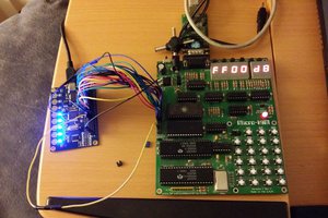
 Jac Goudsmit
 SHAOS
SHAOS
 Justin R.