 Dave Collins
The Rev3 Board is basically a copy of the hand wired Rev2, itself a retrofit HB6809. The Hand wired prototype (see below) was more or less the new chip set design, along with a very stable pierce oscillator I built in about 2 weeks time working nights. What was accomplished with the REV2 build was considerably faster clock, which clocks both the 63C09 and the AVR simultaneously at 16 Mhz. The plan is to push the Rev3 to 20 Mhz. In order to do this it was clear I had to make some tough choices about the chip set. Looking back at the failings of the REV1 board, one of the biggest issues was chip count and latency. These things didn't matter as much on the breadboard prototype as it ran an asynchronous clock (similar to the Z80-MBC2) with the AVR clock coming from a crystal oscillator, and the AVR it's self clocking the 63C09 at 1/4 to 1/2 it's clock. But when I translated that design it didn't seem to work well on the PCB. This coupled with several mistakes made while documenting the Big mess of wires breadboard, and in the actual routing mistakes the whole board was more or less a non starter.
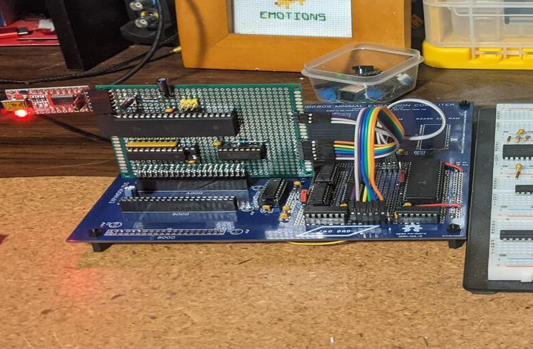
What I learned from the REV1 board is to fit all of these components comfortably on a Mini ITX motherboard, I needed to reduce the chip count to make all of the connections fit (or go to a significantly more expensive multi-layer board). In order to do this I had to significantly reduce the chip count, and in the case of the bank selection circuitry I further reduced the space the chips take up by both simplifying the the design and choosing different parts. A few of you have commented that it might be simpler to just roll together a custom ULA for the design. I think that this makes a lot of sense, but the trouble with that approach is that it may become harder to find CPLD / GAL parts as replacements. This is not the case using standard 74 series parts, and as you will see below the design is very simplified to what I could determine as the fewest possible parts to accomplish what was needed.
New memory map:
The simplified memory map made using less logic chips for address decoding significantly more obtainable.
| ROM / RAM Configuration | |
| Addreses | 64K Main Address Space |
| B000-FFFF | Upper Fixed Ram 20K Physical Rom Space ( |
| A000-AFFF | Device Address Space for MCU and Mezzanine connection |
| 4000-9FFF | Lower Fixed 24K Fixed Lower Ram Bank |
| 0000-3FFF | Memory Bank Window, set by bank register (16K) |
| 128K RAM Chip Layout | |
| 1C000-1FFFF | Bank 7 (16K) |
| 18000-1BFFF | Bank 6 (16K) |
| 14000-17FFF | Bank 5 (16K) |
| 10000-13FFF | Bank 4 (16K) |
| C000-FFFF | Bank 3 (16K) |
| A000-BFFF | Bank 2 Usable – 8K of usable space 2000-3FFF in bank address |
| 8000-9FFF | Bank 2 Lower Fixed Ram Bank top 8K of Memory “Shadow” |
| 4000-7FFF | Bank 1 Lower Fixed Ram bank bottom 16K |
| 0000-3FFF | Bank 0 (16K) system boots with this bank loaded giving 40k cont. |
“Bank2” selects the ram chip between 8000-BFFF. When this bank is selected, 0000-1FFF (in the bank) will map to the last 8K of the fixed RAM area (in the 64k address space of the CPU). Whereas 2000-3FFF is available for use for programs. Overwriting the bottom 8K will cause data corruption in the top of the fixed RAM area (in the 64k address space of the CPU), As this is effectively the same area on the ram chip.
In “RAM Only mode” the address range B000 – FFFF is physically writable at that CPU physical address as the ROM is disabled. This can be configured on the board by removing the “ROM Enable” jumper
and moving the Ram selection Jumper to “RAM” In this mode the AVR needs to be configured to update the ram from SD at boot. This is not yet implemented
The bank selection circuit was simplified greatly and reduced from 3 chips to 2, using more or less the same circuit as before for address decode. With the added benefit of being able to relocate the system page and various other stacks, along with the reset vectors being hard coded to the top of memory this makes placing the swap-able memory bank at the bottom of RAM ideal so long as the programmer is careful to not swap the various stacks from accessible space.
Bank select chips:
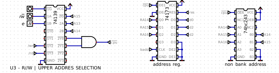
Bank selection is handled by a 74hc173 (4 bit register) and a 74hc243 (4 bit bus transceiver). Output selection is determined by one half of a 74hc139 (dual 2:4 decoder) and 1/4 of a quad and gate, used to AND the two values from the address decoder and generate the /CPU signal. Each chip is able to tri-state its outputs which are hardwired to the top of the ram chip address lines A14,A15,and A16. While the 243 is set up to output the CPU physical A14 and A15 lines (and hold A16 low) when /CPU is HIGH, the 173 is configured to output its stored logical address values (at the same locations) when /CPU is LOW. The stored value is clocked from the bus with the actual clock signal being driven by a AVR request. Simply writing to an address mapped to the AVR (which sees the bottom 4 address lines) will trigger to the AVR to send a clock signal to the register, which will latch the bank address logical value into the register. (currently implemented and verified working)
The address decoder / request grant circuit:
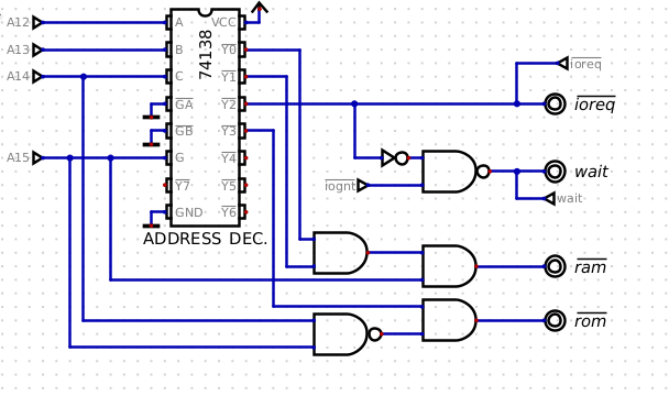
The address decode circuit uses a single 74hc138 3:8 decoder (just like the HB6809), the remaining 3/4ths 74hc08 quad AND gate, and 1/4th of a 74hc00 NAND gate. The logical function of the /ram, /rom and /ioreq signals are fairly self explanatory following the logic gates. The request grant circuit is a single inverter from a 74hc04, and a 1/4th of the NAND gate. This is the same Request grant circuit that is used in REV1. Essentially wait is driven low by sending y2 from the decoder to a low state by writing or reading from the address range A000 - AFFF. Wait is sent to a buffer which has it's output connected to MRDY on the 63C09. This causes the clock to stretch. Meanwhile the /iognt signal is controlled by the AVR, the AVR holds this signal high, until an IO operation is confirmed "done" and then it sends it low for exactly the same period as 1/2 system clock (a benefit of the now synchronized clocks). This is the exact amount of time required to hold wait high until the address cycle has moved on to the next in the 63C09. Some degree of care needs to be taken to assure that the AVR does not stretch the clock for "too long" which is defined by the datasheet as approximately 6uS. It is important to understand once /iognt is asserted the clock stretch immediately ends and the internal registers and instantly refreshed on the falling edge of E (which happens at roughly the same time as the MRDY signal is returned to a high state)
Tri-state buffer:
The sixth and final chip is a 74HC125 Tri state buffer. This chip handles the various signals such as the IO request signal in the case of a mezzanine request, the various read and write signals as well as holding the MRDY signal in a high state during system reset (as the grant circuit is not configured by the AVR during a system reset).
Next steps:
Next is waiting on boards from PCBWay which should come next week some time, I still have to spend some time testing a few things on the REV2 board in the meanwhile such as handling the mezzanine requests. The eagle eyed among you will have noticed that AVR has to do some work to roll over the grant signal in this case. Once the boards arrive, some time must be spent putting them together and testing the additional features. One of my concerns is handling the SD card requests in a timely manor during the 6uS window. I have a few ideas for this but would be interested in hearing someone else's take on that. Once I have the SD card up and working I will need to work on a bootstrap loader for the RAM only mode of the board -- this will involve writing a small machine language program that can be handed off to the CPU at boot time one byte at a time - this is exactly how it is done on the Z80-MBC2 and can be done in almost the same way on the 63C09.
Discussions
Become a Hackaday.io Member
Create an account to leave a comment. Already have an account? Log In.