 Jim Jagielski
Intro
I came across the various Ben Eaters 6502 Computer videos and addition to being impressed with his style, skill and knowledge, I also became intrigued. Back as an undergrad at JHU, one of my courses was in microprocessor architecture, and a project was a 6502 breadboard setup. I can't recall the full specifics; I am pretty sure that other than RAM and ROM (maybe 8k of each), there were no other 6502-family chips used in the project. Just some logic gates, switches and LEDs. Still, I had a blast with the project and took my time to plan every detail, both from a hardware placement standpoint to software design. When all was done, I was extremely proud of what I did and was also shocked when the Prof was just as impressed. He kept my wirewrap (no pushboards back then) and code as a prototype example for display in the course.
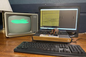
My first computer was, as with many, an Apple ][, which was also 6502 based, and I spent many, many, many hours coding on that, in both assembly and Basic. The skills I learned doing assembly language programming are still valuable to this day.
So when I saw Ben's videos, I was hooked. I decided to work on my own version... Here you go. All code and examples are available under permissive Open Source licenses, so please don't hesitate to use, and re-use, what you need.
Project Guidelines:
I'll be focusing on the 65C02 and its companion chips (eg: the 6522). Also, as much as possible, I'll make things as generic as possible so even if your design differs from mine, there will still be a lot that you can use, re-use or hack. I'll use more contemporary chips and solutions where it makes the design significantly more elegant, but won't let that over-shadow the actual retro nature of the project.


 Johannes le Roux
 Bernhard "HotKey" Slawik
 Justin Skists
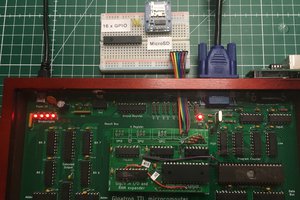
 Marcel van Kervinck
I'm looking forward to seeing a schematic update with the RP2040 included in the design.