 Shih Wei Chieh
Manufacturing of Large Dye Sensitized Solar Cell at home from Shih Wei Chieh on Vimeo.
Introduction
Dye-sensitized solar cells (DSSCs) represent an easily manufacturable and cost-effective photovoltaic device and can be done at DIY level. However, its efficiency remains relatively low, posing challenges in meeting commercial standards, primarily due to limitations imposed by the limited conductivity of the FTO or ITO layer within the system. DSSCs offer the advantage of highly customizable patterns and colors for a transparent TiO2 layer, providing opportunities for aesthetically pleasing smart surface designs and is electrically self sufficient. Chemicals utilized in the experiment are mostly purchased from Greatcell Solar, therefore, most of the processes are conventional except the size of the cell in this experiment. The efficiency is about ~5.8V and ~51mA. The low current performance is due to the absence of the parallel circuit here.
1. Experiment
1.1 Etching the series circuit on FTO glass
To achieve the necessary voltage, a series circuit is needed to be created with the glass substrates. To achieve this goal, the FTO glass needs to be etched, to create a vertically connection between two FTO glasses. The first picture below illustrates the cross-section of the structure and the positioning of the 12 cells.
About the chemicals employed in this section, firstly, adding 26.3 mL of 38% hydrochloric acid solution to a beaker and then dilute it with water to reach a total volume of 100 mL, to make a 2M HCL solution. The wet photoresist I used here is a product LP8901V6 purchased from Great Eastern Resins Industrial Co. Ltd.(GRECO).
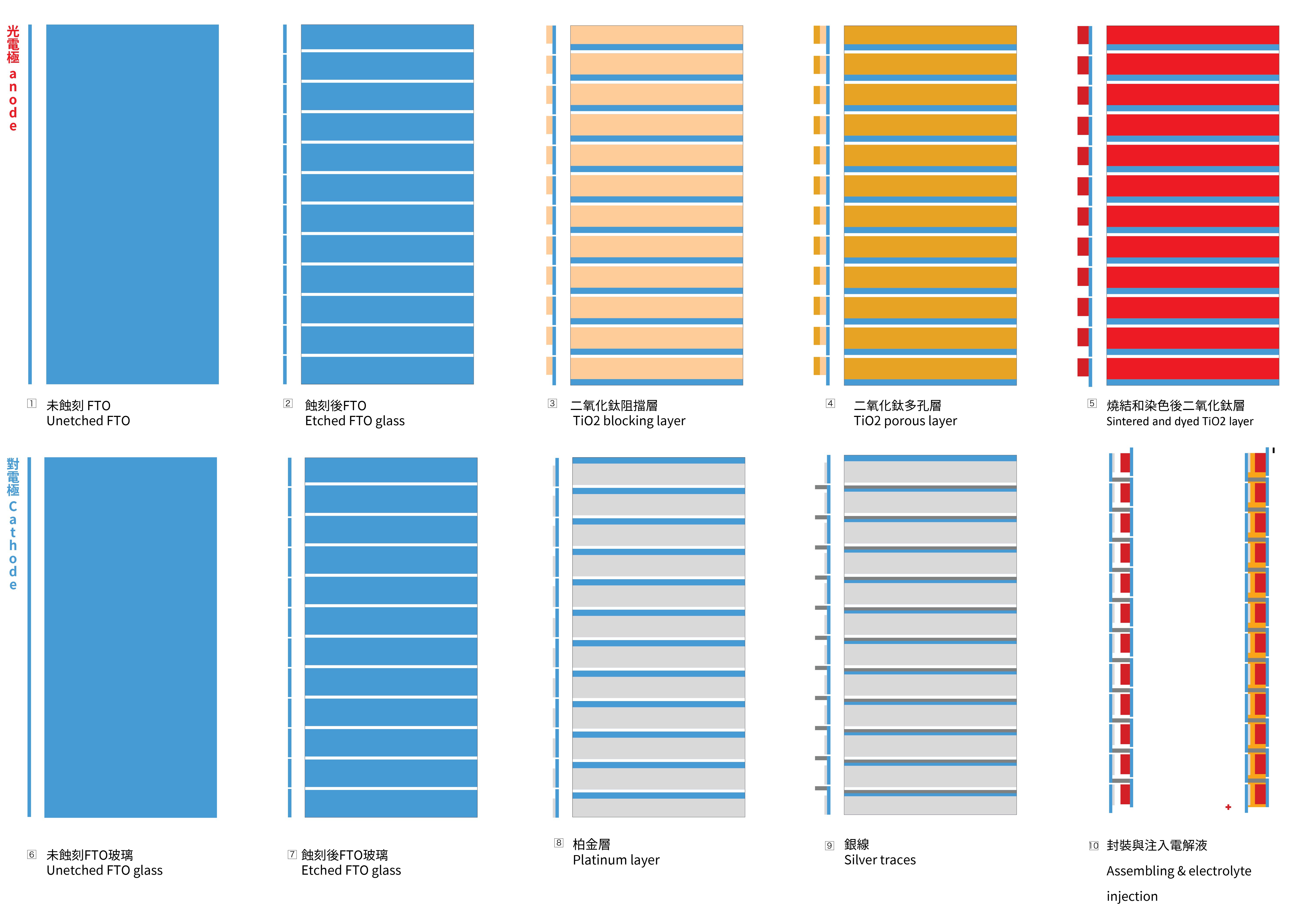
1.2 Sintering of the blocking TiO2 layer and porous TiO2 layer on the photo-electrode
- Apply Kapton tape to the glass to create the mask for the TiO2 layer coating.
- Apply the BL-1 paste with a glass coater. This mask will be shared to make the porous layer later.
- Place the photo-electrode in the kiln, ramping up to 125ºC at a rate of 8ºC per minute without removing the Kapton masks. Maintain this temperature for 30 minutes, and then allow it to cool naturally to room temperature.
- Take the cooled glass out and coat the glass again with with 18NR-T paste with a glass coater to make the porous TiO2 layer, then fire it with a ramp rate of 8 ºC per minute to 450ºC. Keep it at 450ºC for 30 minutes before allowing it to cool down naturally to room temperature.
 Josh Starnes
 Scott Clandinin
 Theresa