 Kelvin Brammer
Several years ago, I had to learn how to use National Instruments Circuit Design Suite (Multisim and Ultiboard) to create a circuit schematic and PCB layout for a new job. This was so that I could better understand the software, and help students with the process of creating a schematic and converting it to a PCB. I would then manufacture their PCBs, and then give the board back to the students to build . To help learn this software, I decided to make a fully functional 555 timer from 2N3904 and 2N3906 transistors.
I decided to follow a schematic that also laid out the components in to there specific functions, e.g. Threshold Comparator, Trigger Comparator, Flip Flop, Reset/Discharge, and Output. It could then also be used as a demo board in labs.
We used a LPKF S63 PCB milling machine to create the PCBs, so I also had to learn how to export Gerber files, and the idiosyncrasies of the software that runs the S63. Happy days.
The complete PCB also had a ribbon cable attached so that it could plugged into any socket instead of an actual 555 timer IC.
Several years later, I had to repeat this process to learn Proteus. Proteus was introduced so that we could also simulate PIC microcontrollers in the circuit schematic (incorporating C code or hex file). I decided to repeat the creation of the 555 transistor circuit.
I have recently discovered Hackaday, and started to listen to the podcasts starting at the beginning with episode 0, and listening to them in order. I don't fully comprehend what some of the projects, quick hacks, and articles are talking about, but ABSOLUTELY enjoy listening to them, and reading the articles I do get. So far I have correctly guessed 5 of the "Name That Sound", but as I have not been listening to them in real time, I have not been able to enter.
I had been thinking about making another 555 timer PCB, but one such that the PCB itself said 555. One Hackaday article, "Smallest Discrete Transistor 555 Timer" by Tiny Transistors, inspired me to attempt something similar, but using SMD parts.
I decided to also make a small 8 pin adapter board so that my 555 PCB would stand up proudly from any circuit it was plugged in to. The actual PCB layout for the 555 itself had to be done several times. Initially I thought about making the 555 board 60mm wide. I exported a DXF from AutoCAD for the board outline. However, as I had chosen to use the same size components as Tiny Transistors board, there was a lot empty space. I resized the board down to 30mm and tried again. But this time there was not enough space to route the traces. I finally ended up with a board 42mm wide.
Whilst I am fully capable of assembling this board, SMD parts and all, I also wanted to learn the process of of getting JLCPCB to populate the board, tweaking the Bill of Materials such that my parts matched theirs. This took a bit of time, trying to find the right page on the website that listed their stock and part numbers.
But within 2 weeks of placing the order, my boards were delivered. All I had to do was mount the PCB vertically on the adapter and add some headers.
I think it looks amazing, but I am biased.


 Jefferson Bueno
 Benchoff
 Dave's Dev Lab
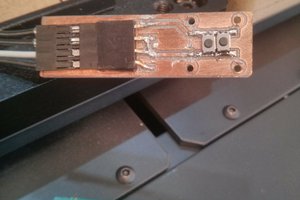
 brainstorm
Fantastic! Love the look, and the fact that it's a plug-in replacement is very cool.
Wrote this up for the blog, should publish soon. Thanks for tipping us off!