 helge
helgeAlright, this project definitely got some love today. That PCB is really not that great (as in: damn that DDC118 is super sensitive).
Changes (3 years in the making ^^):
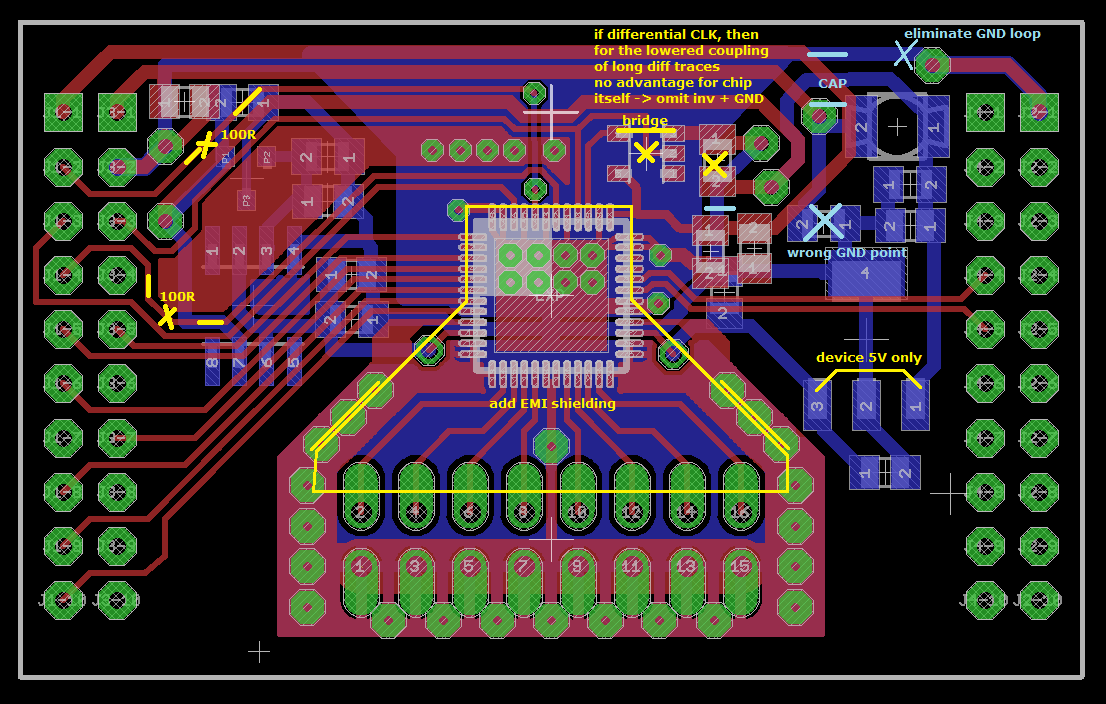
- add missing bypass caps, mostly 220nF ones, test direct bypass to AGND polygon (no significant change from the latter)
- insert 100R clock termination resistors for T2CCP1 (@2.5 MHz) and DCLK (@10 MHz)
- insert 22R in the trace supplying the voltage reference -> no significant change (not shown in layout changes)
- insert 10k series resistance on REF3040 output -> no significant change (not shown in layout changes)
- omit 74AHC1G14 single schmitt inverter. I had re-routed the cap next to it for proper 3.3V bypass including 10R resistor to the caps below but no improvement was evident. A differential clock source only really shines on larger PCBs and flex cables.
- see that cap between the second trace on the top and the LDO tab pad where it says "wrong GND point"? That cap was moved upwards because connecting it to the bypass caps behind the filter would only couple noise from the input to the output. The two traces on the top right are static and don't couple much noise into the rails.
- add EMI shielding (tin coated sheet metal cut to size) above the chip and sensitive traces. That did away with a good fraction of the 50 Hz line perturbations which are superbly evident at 100 samples/sec. The A (B) side samples themselves are supposed to be rather consistent but showed slow beating without the shield. Additionally the noise introduced by an approaching hand is mostly gone without anything connected to the inputs.
Code changes:
- endianness issue resolved, both 16 bit and 20bit modes look good
- right now both integrator sides are being printed, looking good at 400 samples/sec but that might get worse as integration time is increased due to differences in the capacitances and active analog front end circuitry
- SPI speed changed to 10 MHz

Next: There's a hint regarding noise performance. For best performance the CONV transition needs to happen within +/-10ns around a T2CCP1 rising edge. Right now CONV is generated from within an ISR which has delay and jitter.
This may possibly be solved by routing a trace from a T1CCPx pin to CONV and subsequent configuration of both timers. All timers have pre-scalers and can be synchronized to some extent. Not sure what cases can crop up though. Maybe It's best to latch CONV with T2CCP1 and keep the interrupt based scheme.
NC7SZ175P6X looks right for the job.
In summary, ditching the schmitt inverter for !DCLK (which likely inejcted more noise than help reject transients) and adding the E field shielding did a lot to improve performance whereas it is hard to tell apart what that course of ground re-routing and bypassing actually did. Maybe it wasn't that big a deal to begin with. Powering the Launchpad + DDC118 externally and testing it with floating pot. laptop showed no difference.
Discussions
Become a Hackaday.io Member
Create an account to leave a comment. Already have an account? Log In.