Yann Guidon / YGDES
-
Cascading the LZB
04/06/2018 at 07:58 • 0 commentsLZB is "Leading Zero Blank" and it's a tiny visual feature that eases reading. When the most significant bits are cleared, the corresponding 7-segments digits are not turned on. I introduced this option in #DYPLED but I guess it existed long before that.
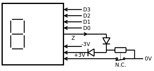
The first project that uses these display modules is #YGREC8 which is 8-bits wide, or only 2 digits. In this case, there is no real cascading. The circuit is very simple : the Zero output is tied to +3V when the input code is 0000, so this powers a relay coil (though a diode). The relay is "normally closed" and connects the 0V rail to the module. So when the input code is 0000, the relay opens and disables the display of the digit "0".
![]()
At first I wanted to mount that relay on the module. Then I decided that the circuit should be on the backplane because each module would need a special assembly, depending on their position.
The good news here is that the overall current is reasonable : the 6 segments draw about 13mA×6=80mA, OR max. 60mA for the coil (which cuts the 80mA when activated). Using a prebias resistor, this can be reduced a bit (at the price of more static consumption). So a spike would draw maybe 60+80=140mA, or 200mA worst case, and the two other relays in the decoding tree will not suffer too much.
(If you missed one episode, the RES15's contacts are rated at about 100mA)
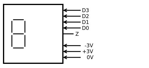
This was the description of the wiring for the Most Significant Digit. The Least Significant Digit doesn't use a relay because its digit is always on, and its wiring is more straight-forward:
![]()
So a 8-bit bus requires 2 modules, as well as 2 diodes (one for freewheeling to the 3V rail) and one relay on the backplane.
For more bits, it gets a bit more complicated. In the case of 16 bits, 4 digits are required. The MSB looks like the first diagram and the LSB is like the 2nd diagram. The two other digits need more sophistication...
-
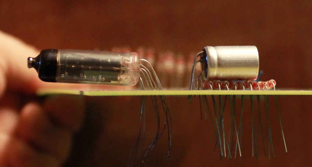
PCB prototype
04/05/2018 at 16:37 • 1 commentJust a quick update.
The PCB prototypes was just finished, supported by # Lets make OSHW more successful! .
The boards has been sent out to Yann Guidon / YGDES who insisted to do the assembly. Here is your sneak peek at what the board looks like before assembly:
![]()
-
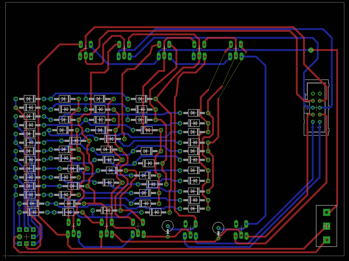
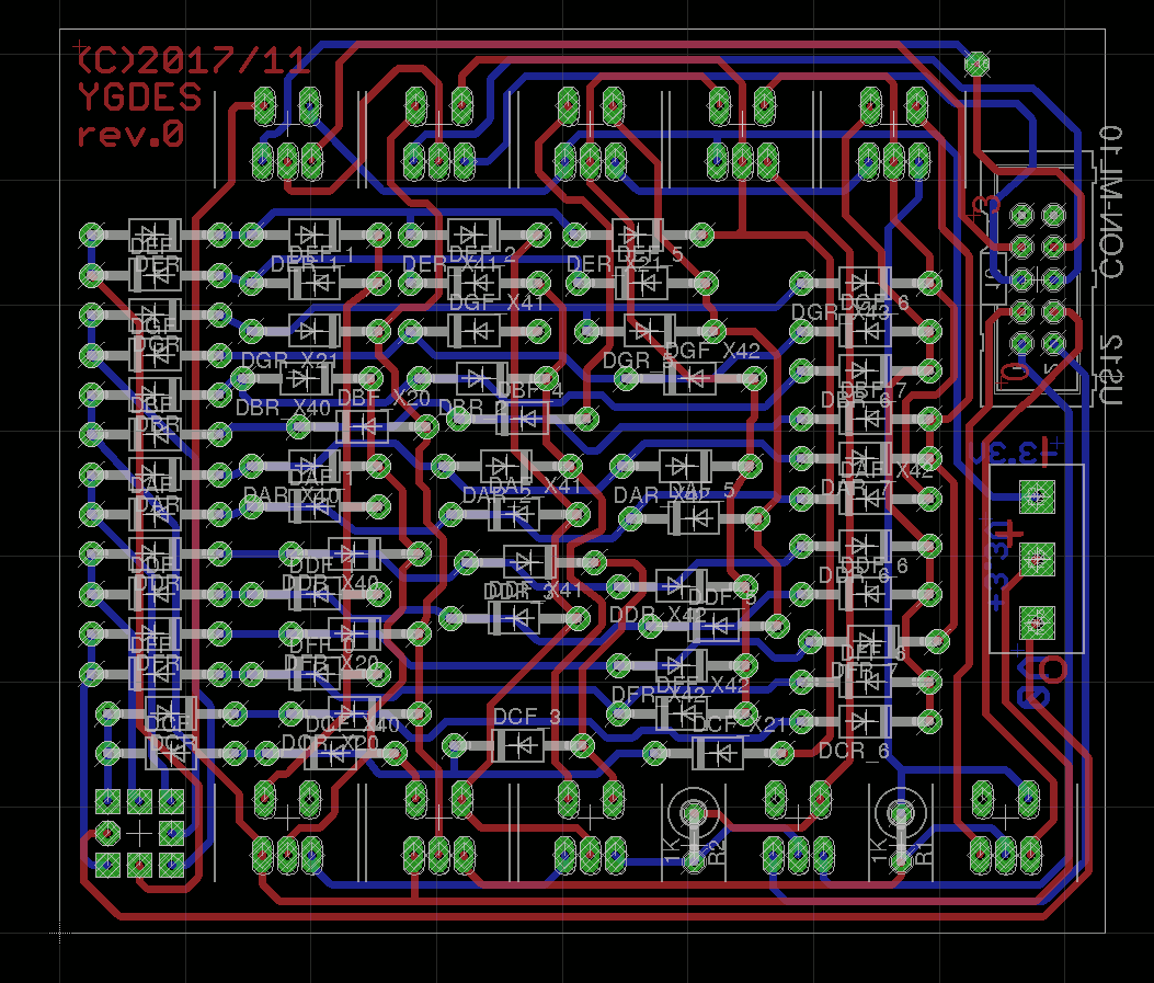
New layout
03/28/2018 at 04:38 • 0 commentsI've spent the whole night polishing the new version (Rev.1) of the PCB.
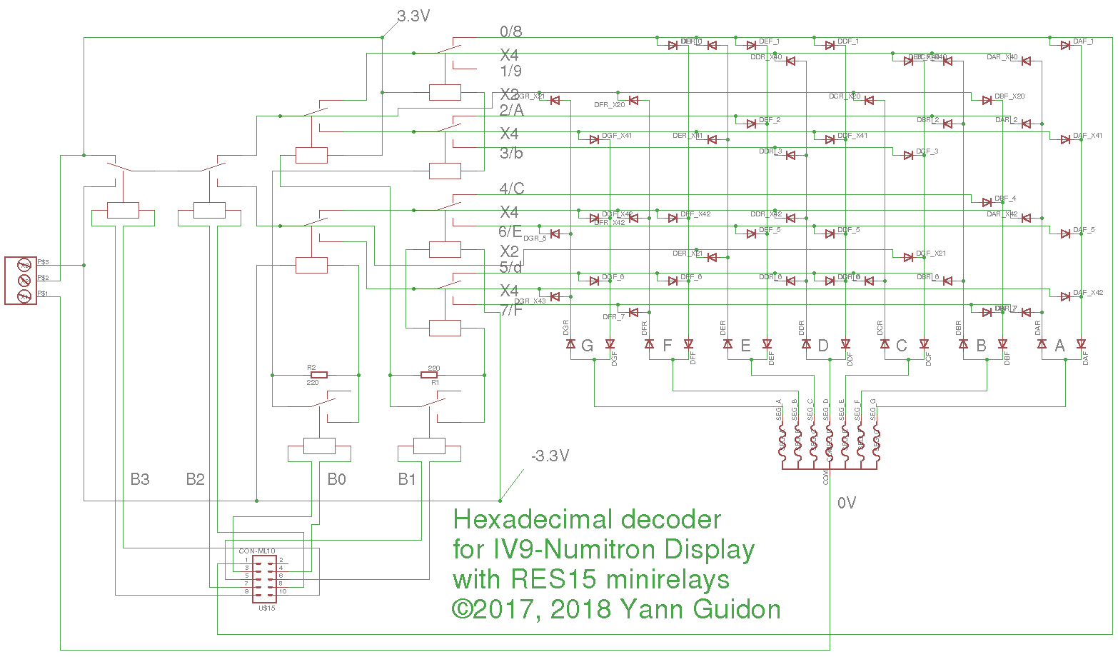
I iterated a lot and finally, I only output one more signal that is tied to +3.3V when the input code is 0000. Cascading is easier and totally optional, the backplane must do its own circuit depending on the desired behaviour and cascade length.
![]()
The layout finally contains three mounting holes (3mm diameter) and several things have been moved around. You'll notice the crossed transistor symbol ;-)
![]()
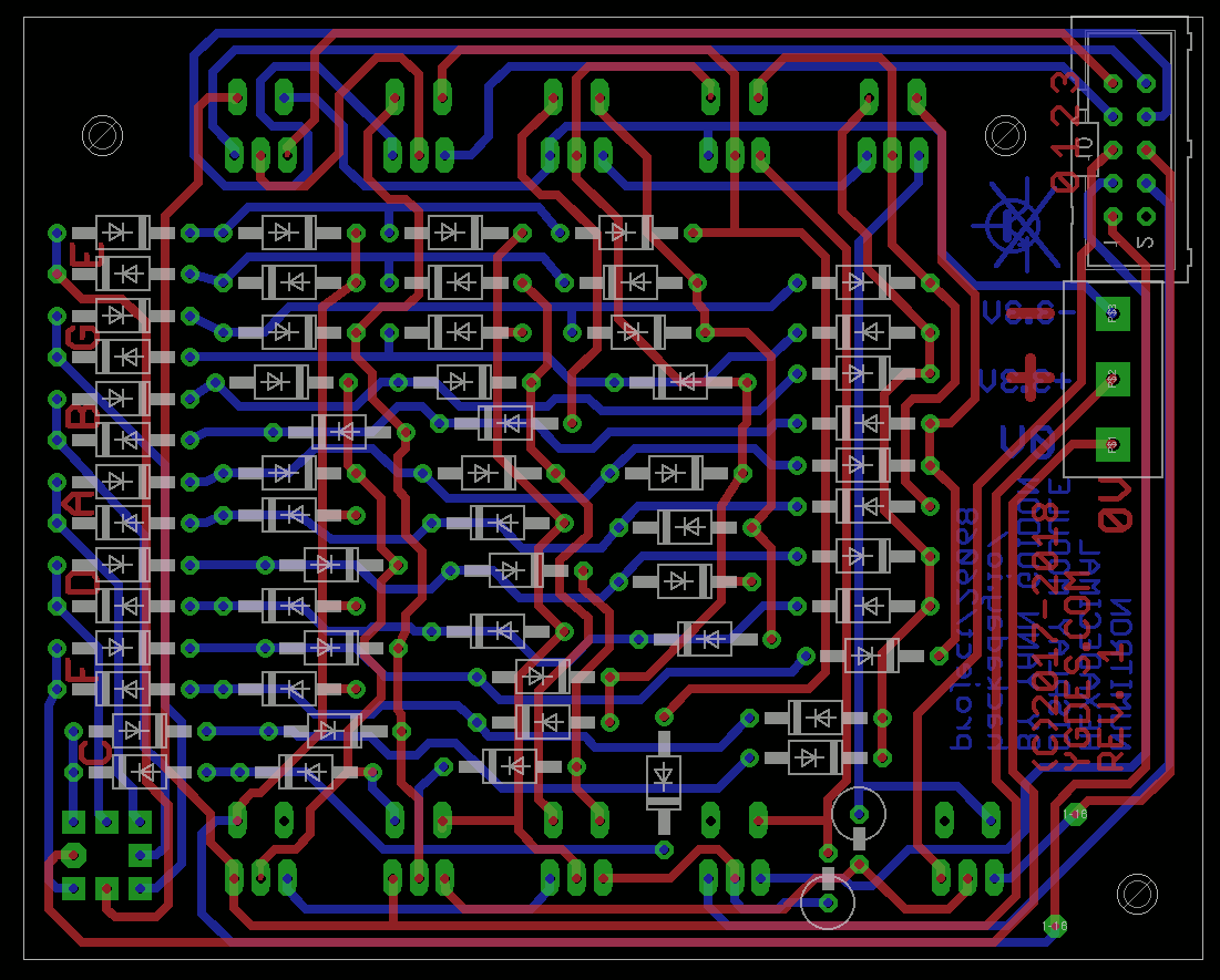
Dimensions are 90×72mm. I have removed one via but 2 new ones have been required in the end.
The layout is VERY conservative. No silkscreen is needed, all the necessary information is available on the copper. For example the pad shape of the diodes are octogonal at the cathode end. The idea is to create the boards with old technology (even on bakelite :-D) so even the lousiest fab should work.
I'll have to figure out the orientation of the IV9 tube... There was a little issue with the footprint but nothing critical.
Anyway, the board is looking good®, it allows blanking-cascading and (I just realised) the single-relay input allows these relays to be used as hysteretic data storage...
-
Enhancements
03/25/2018 at 23:59 • 0 commentsI would like to build a working unit for the Hackaday Prize 2018 but other projects have taken precedence... #YGREC8 has progressed a lot :-) But the Numitron display is almost done, there is not much left to do, before I get a functional pre-series module, so why not do it now ?
I stopped just before sending the boards to fab because an astute observer noticed that I forgot (again) to include the mounting holes. And I had already finished routing the board...
Another consideration is directly derived from 5. BLANK : the modules should be cascadable and the most-significant 0s should be blanked. This means that the circuit must have a blank input and blank output signal.
Blanking the digit is easy. Just insert a relay in series with the 0V common rail (normally open or normally closed, as you like). This could be done on a backplane where several digits are connected.
Cascading is different because the coils require so much current and the circuit has not been designed for this dual purpose. The cascade needs to do a OR (or AND) of 4 inputs (detect the input=0000) and it's already using many relays.
One approach is to extract the corresponding signal at the 0/8 node, at the leaf of the binary tree, but it also drives 6 segments (15mA each) so the overall current is already at the limit of the tree relay's handling capacity. I don't want to fry the contacts.
Should I just leave the proto as is and send it to fab so I can test the additional circuit during its fabrication ?
Oh and let's not forget @Fredrik Högberg who started # Lets make OSHW more successful! He'll handle the PCB fab part. Thanks !
-
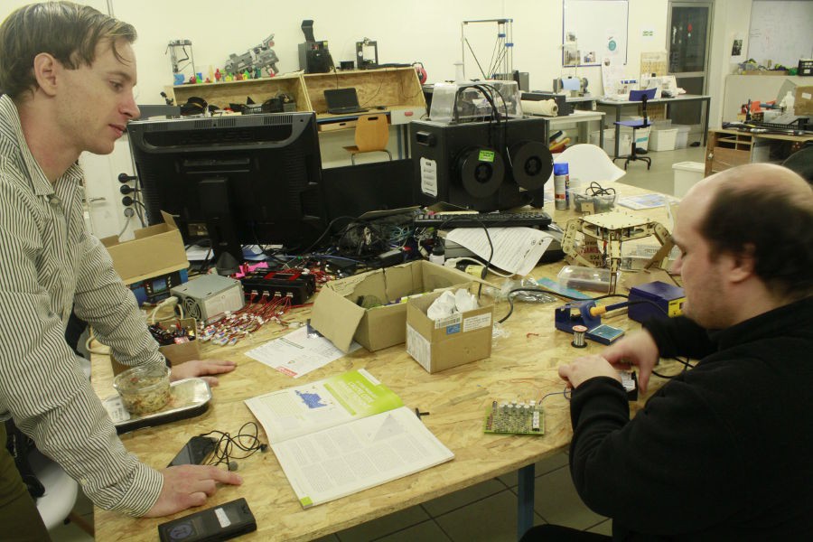
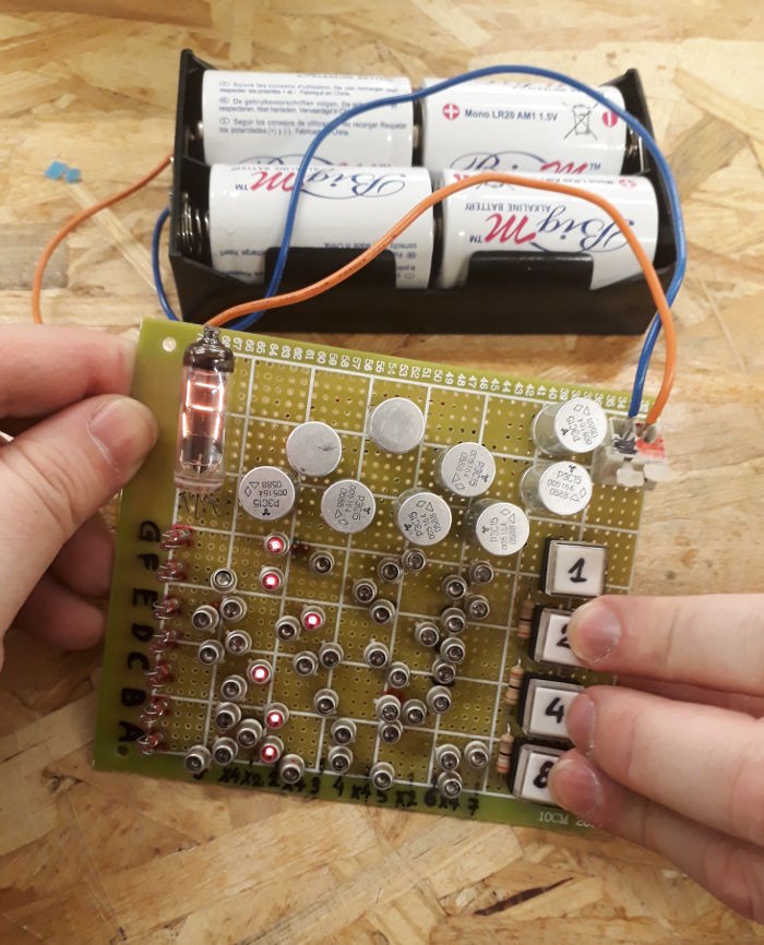
The demonstrator goes portable !
11/29/2017 at 13:29 • 0 commentsI'm currently traveling in France and showing the module to other hackers and others !
However I've always used the demo board with my lab PSU so I need a cordless, portable power supply. I designed the module to accommodate 6V, or 4× alcaline cells, instead of 2×3.3V.
Just before leaving, I had a bad surprise : the circuit draws so much that AA batteries simply can't supply enough current. The device almost shuts down when buttons are pressed. With the lab PSU, I saw that it wouldn't work well at 5.9 or 5.8V and the AA batteries are too weak...
I arrived in Toulouse to visit @VDagrain, who loves that kind of hack, so I bought four C-type batteries, and visited "Le comptoir du Languedoc" to buy a suitable holder. Then, we visited the Artilect hacklab to solder that together.
![]()
(thanks Alexis !)
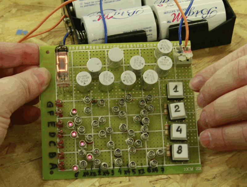
There was a bad contact in the battery holder but now it works nicely ! It's more bulky but the stunned gaze of people is really worth it :-D
![]()
Thank you Wanda ;-)
![]()
:-)
-
PCB
11/06/2017 at 02:02 • 0 comments![]()
The layout looks great ! I'm preparing it for fabrication, but I want to add some extras in the batch, for a side-project...
-
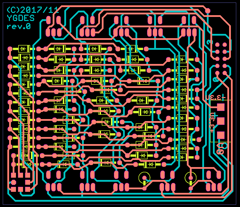
Beyond the prototypes
11/02/2017 at 15:08 • 0 commentsNow that the principles are working and well understood, it's time to make a PCB.
![]()
The diode ROM uses a bit more space than I initially thought but I managed to keep it pretty compact. However the issue occurs in the other dimension: the diodes add about 3mm of thickness to the stack.
![]()
The IV9's diameter is 10.5mm while the RES15 is 11mm. Add the diodes, the PCB thickness and the unavoidable clearance to prevent shorting the diodes' leads to the next board's RES15 metallic can, and the board pitch is 18mm. So each IV9 is separated by a 8mm gap...
Anyway I've decided to move forward and try to run a first layout through @oshpark (Thanks guys !) before I build a few dozens of modules. I might have to buy a few more thousands of diodes though :-D
The PCB is just a bit larger than 8cm and a little over 7cm high. Enjoy the view !
![]()
The approach is a bit modified : either the module is used "standalone", or the outputs can be broken out to a more conventional display panel (with a smaller pitch for a nice aspect). The connector shapes are temporary but should work nicely for the first attemps.
I am excited to receive the first purple boards :-D Notice however that I have routed the board as if I had to etch it myself or with DIY, lousy resolution, processes. Just like "in the old good days" of perchlo baths with dubious concentration and temperature. I'm ashamed to ask @oshpark to build these because I wanted to use their high quality process... But I couldn't wait this time.
-
A new ROM layout generation script
10/30/2017 at 17:28 • 0 commentsI have just uploaded convo7seg_09.html which computes the ROM configuration from the updated digits.
As I wrote in a previous log, the lines 5 and 6 must be swapped, or the output is totally messy. The swap must be integrated in the initial array, not at the line drivers level. This new script confirms the configuration that is implemented in the 2nd prototype.
Here is the output :
...v^v.v.....v  0/8
......^..v^.^.  X4
..............  1/9  <- empty line :-)

^.^.....^..v..  X2

.....v....^.^.  2/A
.v..^..v.....v  X4
......^..v....  3/b

...........v..  4/C
.v^v..^.....^.  X4
^....v.v.....v  5(6)/E

....^....v....  X2

.v.v..^v^.^...  6(5)/d
^............v  X4
..^........v^.  7/F

Total: 45 diodes
-
Second valid prototype
10/26/2017 at 01:30 • 0 commentsPrototype #2 works !
Time to learn French ;-)
Please note that this is a "demonstration unit" that uses a slightly different driving topology because the LED require higher voltages. The LED are only intended to show off (aesthetics matter !) and the series units will use the intended "dumb" germanium diodes.
The design of the diode array is now "right", the concept is validated and CAD should begin... "soonish".
-
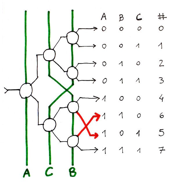
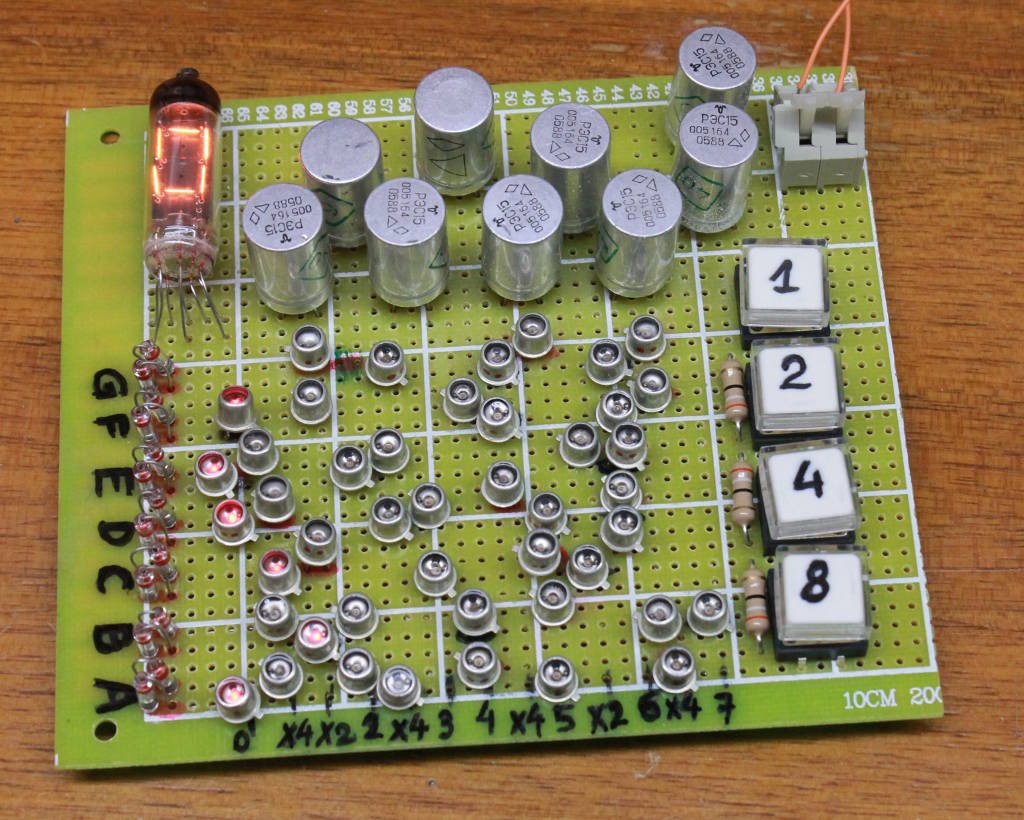
Another mistake
10/24/2017 at 23:52 • 2 commentsDo you remember this picture from the last log ?
![]()
OK and now, let's think again about how the diode matrix was optimised.
The short version is : the digits 5, 6, D and E are bork.![]()
This means that my carefully optimised diode matrix is invalid. I have to swap 6 and 5 before optimising to preserve coherence...
The swapped array:

^ ^v^v^v^v^v^v (0, 8)
^ ^   ^ ^v^v^  (1, 9)
^v^ ^v v^ ^v^v (2, A)
^v^ ^ ^v^v v v (3, B)
 v^v^ ^  v v^  (4, C)
^v^v^v^v v  ^v (6, E) \ swap !
^v v^ ^v^v^  v (5, D) /
^ ^ ^    v v^v (7, F)

The new optimised array :

   v^v v     v (0, 8)
      ^  v^ ^     X4
^ ^     ^  v      X2
     v    ^ ^  (2, A)
 v  ^  v     v    X4
      ^  v     (3, B)
           v   (4, C)   (2 ^ to remove)*
 v^v  ^     ^     X4   (2 ^ to add on A and F)
^    v v     v (6, E)  (1 v to add and 2 ^ to remove, swap with 5)
    ^    v        X2    (unchanged)
 v v  ^v^ ^    (5, D)  (1 v to remove and 2 ^ to add)
^            v    X4 (2 ^ to remove)
  ^        v^  (7, F)   (2 ^ to add, reusing those of 4)
So I have to rewire quite a few diodes... Half of them in fact ! Well, not really, because some of the changes are rather symmetrical. For example, the X2 line is not changed and instead of removing LEDs from line 4, the LEDs can be rewired to line 7.
This gives you an idea of the rework that awaits me:
![]()
Numitron Hexadecimal display module
Another hexadecimal display, this one is sans transistor for the extra vintage touch, and uses only Soviet-era parts