 Nick Ames
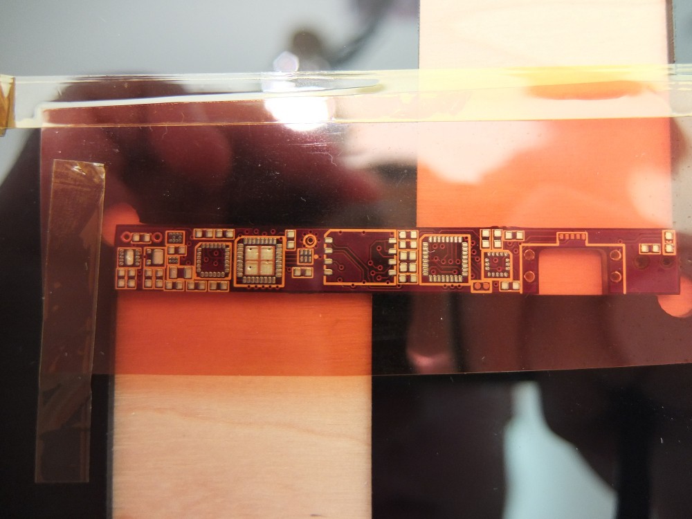
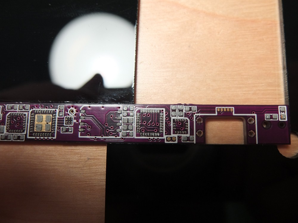
Space is at a premium on the NoteOn PCB. The PCB is only 8.1mm wide, just barely larger than a SOIC package. To make the design fit, I used leadless packages for all the ICs. Most of the chips are QFP or LGA packages. The voltage regulator and battery monitor are chip-scale BGAs.
This was the first time I've used leadless packages on a project, and I was worried that there would be problems with short circuits and dry joints underneath the chips. To my surprise, everything went fine. In this build log, I'll go over the process I used.
My PCBs were purchased from OSHPark. They produce high-quality boards, and their $5/sq. in. price is a fantastic value if your designs are small. .003" Kapton solder paste stencils were ordered from OSHStencils. I purchased a set of their board guides to rest the stencil on.
The boards were stenciled with ChipQuik SMD291SNL lead-free solder paste. I had some issues with paste bridging between pads, so I used a needle to scrape the paste out of the way.
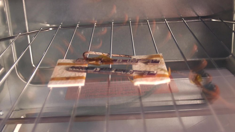
The boards were reflowed in my temperature-controlled convection toaster oven. It's not fancy: a thermocouple and on-off control of the oven are all that's needed. Ideally, the thermocouple would be attached to the board being reflowed, but trying to attach a thermocouple to a board as a dense as the NoteOn PCB would be a recipe for disaster. Instead, I taped the thermocouple to a one of the spare NoteOn PCBs and placed the actual board near it.
Discussions
Become a Hackaday.io Member
Create an account to leave a comment. Already have an account? Log In.