deʃhipu
-
Custom PCB Outline
07/01/2018 at 17:59 • 0 commentsOne of the greatest advantages of Fritzing over other PCB software currently on the market is its ability to SVG files directly, without any need of converting or tracing them. Since it uses SVG internally for anything, it's only natural that the PCB outline is also an SVG file. I'm going to tell you here how I go about making custom PCB outlines.
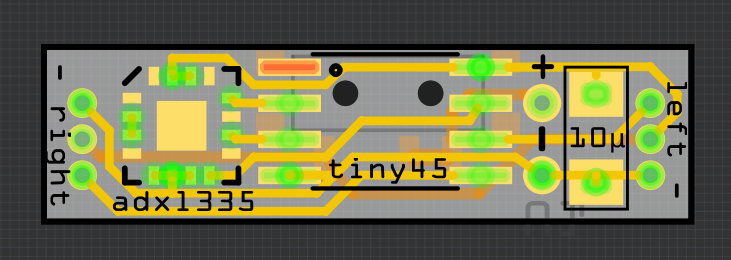
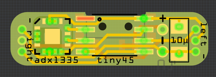
Usually I start by designing everything on a standard rectangular PCB, keeping in mind the rough shape that I am going to need. Here's an improved design for the #Mechatronic Ears with a power switch added:
![]()
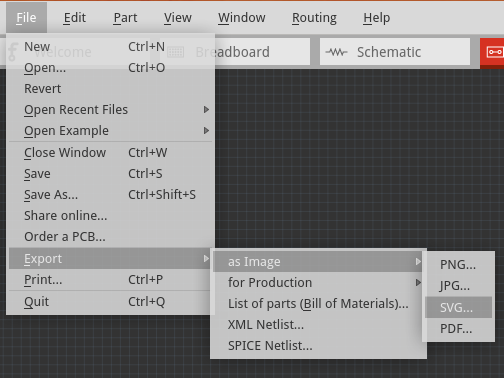
Next, I export the design as an SVG image:
![]()
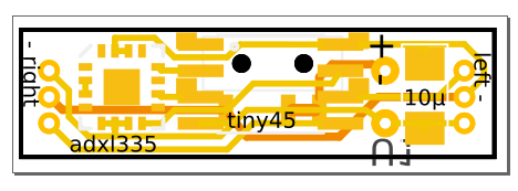
Then I open it in Inkscape, where I can easily draw my desired board outline:
![]()
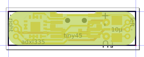
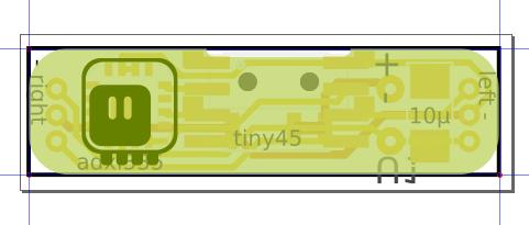
Usually I pick some nice, partially transparent color (green, blue and purple work well) and draw the shape of the PCB I want with it:
![]()
You can also add some silkscreen:
![]()
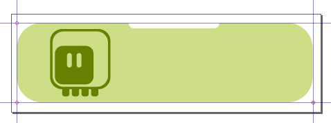
Next, I remove all the Fritzing stuff from the image, and leave only the board outline and the silkscreen:
![]()
Now create a new layer in Inkscape using Layer→Add Layer... menu option, and name it "board". Select the board outline, and then select Layer→Move Selection to Layer..., then select the newly created layer "board". Repeat that with the silkscreen, except call it "silkscreen0" for the bottom, or "silkscreen1" for the top (you can have both).
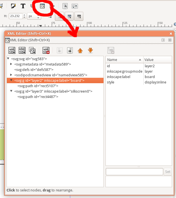
We are almost done. Unfortunately, Inkscape doesn't call the layers the way you tell it — it only adds labels to them with your names. We will need to go a little bit deeper to actually modify the layer IDs. Open the XML Editor, you should see something like this:
![]()
Now you can select each of the layers, select the "id" attribute on the right side, and enter new value for it on the bottom. Change the IDs to "board", "silkscreen0", "silkscreen1", etc. so that they match the labels. Don't forget to click Set each time, or it won't get saved.
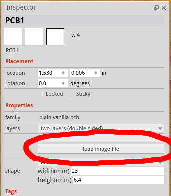
You are done. Now you can save your board as "Plain SVG", and go back to Fritzing. In Fritzing, select the PCB, and in the properties click on the load image file button:
![]()
Select your saved SVG image. You should see a summary telling you how many cutouts (slots) your PCB has — make sure that number is correct. Finally, you will need to adjust the position of your PCB to match the components, and you are done:
![]()
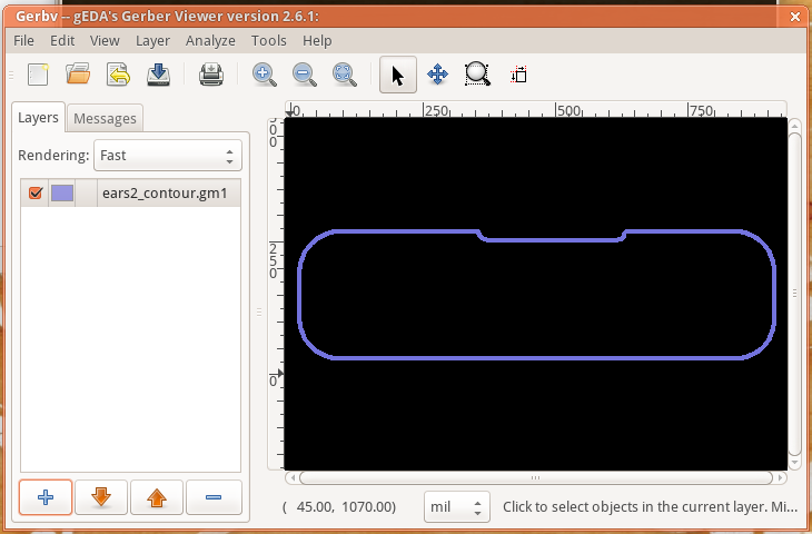
Now, when you export the board as gerbers, I recommend to do one more step before you send it to fabrication: open the board outline in a gerber viewer, such as "gerbv" and verify that the generated shape is indeed correct. Fritzing has some very annoying bugs around the gerber generation, and you might be unpleasantly surprised if you skip this step.
![]()
This time everything is correct. If it wasn't, I would go back to Inkscape and add a couple of nodes to the shape, around the places where something went wrong, to make sure it's correct.
-
Tented Vias
07/02/2018 at 10:22 • 0 commentsThis trick was originally described by @Arduino Enigma in the #Sinclair Scientific Calculator Emulator. Tented vias are vias that are covered with soldermask. If you think about it for a moment, there is really no reason for a via to be exposed (unless you re-use it as a test point). Its job is to connect the layers, and it does it as well when it is covered. On the other hand, when it's covered, the risk of shorting it is smaller, and the board can look much better.
Unfortunately Fritzing doesn't normally give you the option to have the vias tented. But there is a simple trick to add the soldermask over them when you are generating the gerbers. Start by generating your gerber files as usual, and once you do that, select Routing→Select All Vias from the menu, and press the Del key to delete them. It will also delete some of the traces, but don't worry about it. Now generate another set of gerber files, in a separate directory, and close Fritzing without saving the file.
Now all you have to do is to copy the maskTop, maskBottom, silkTop and silkBottom files from the latter directory to the former, and voila, your vias are now covered with soldermask. You can also only copy only some of those files to only have the vias covered on one side of the board.