-
1Step 3: KiCAD pcb editing
There are 4 sub-steps here:
- Import the images to create footprints
- Combine the footprints into one footprint (easier than aligning them in PCBnew)
- Add component (footprint) to PCBnew design
- Add final details to PCB
It is now quite easy to create footprints using the Bitmap2Component editor. However, I ended up repeating my work about 5 times before I figured out how to get the component footprints into the PCBnew design. So I am going to start by explaining libraries and creating a new library, because this is where I had trouble.
KiCAD likes to have the footprints in libraries (makes sense), but you cannot import any old footprint into a design, without it being part of a library first. I hadn't any local libraries created, so I couldn't make my footprints usable.
The steps in order are as follows:
- Create a local library (I made it local to the project)
- Add library to project
- Open footprint editor - set active library to local library
- Open footprint created by bitmap2component
- Save footprint to library
Now the footprint is accessible in PCBnew. Making a new library is explained in great detail here in the sparkfun tutorial.
Now that we have a library to place our footprints in, we can start the actual footprint creation.
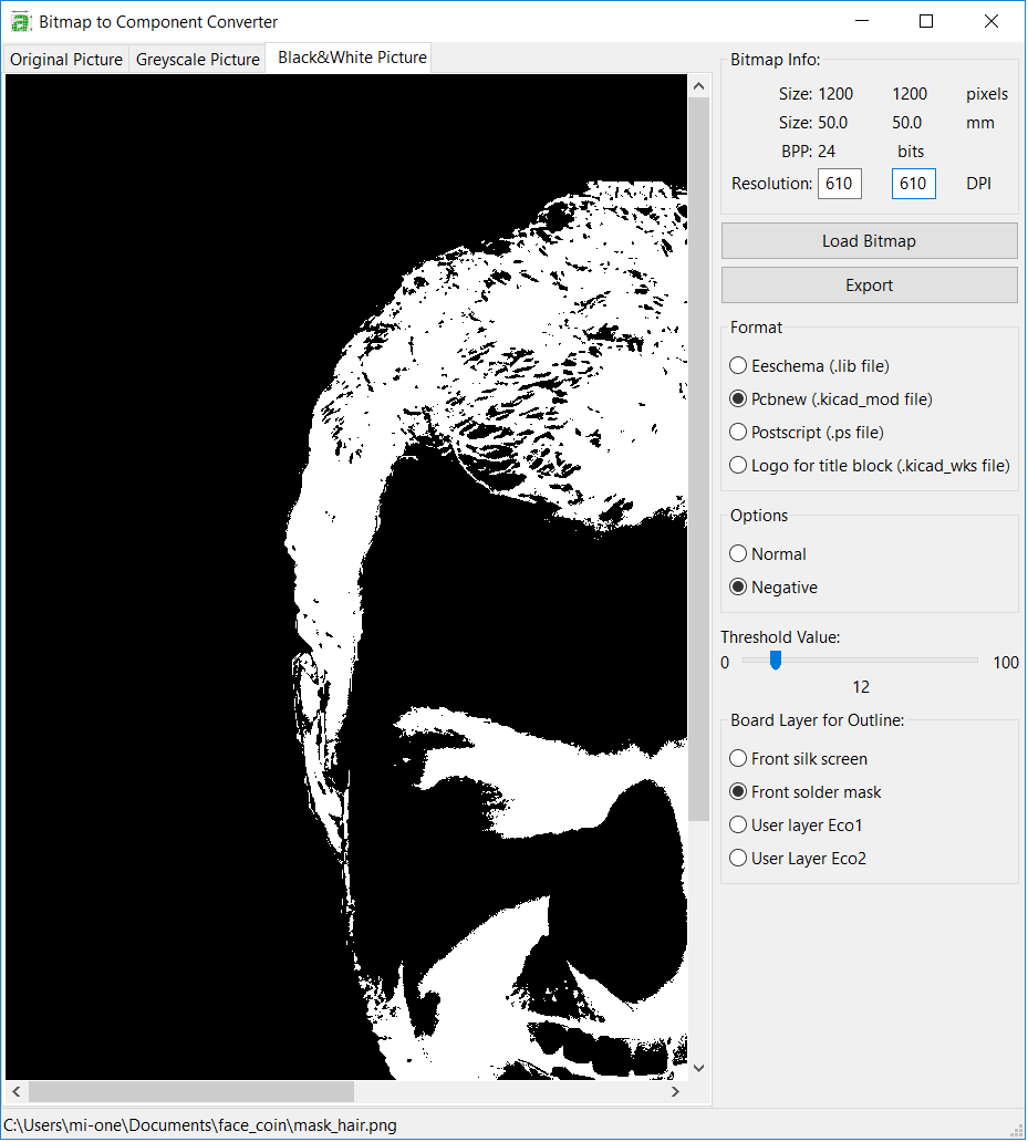
Using bitmap2component, load the first image.
![]()
As you can see in the image, I have changed 4 settings:
- Negative
- Lowered the Threshold
- Creating a Front solder mask
- Resolution 610 dpi
Remember the white is the footprint, so we want everything else to be black. I exported it with the same filename as the image, and the new extension .kicad_mod. Note that the only options for board layers are silkscreen, soldermask and the user eco layers. We will modify them later to create copper layers.
Once this is repeated for all the 4 images, we can now combine them.
Combining them is actually quite easy, once you learn the format of the kicad_mod files. They are a sort of pseudo-xml format, and can be opened in a text editor. The file will contain a 'module', and we want only one module in our final file. I created a new file, and copied the contents of 1 of the files (lets say mask_hair) into it directly. This will be our starting point.
My remaining 3 files are as follows:
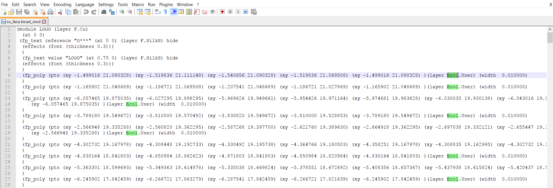
File Current layer Desired layers cu_face eco1.user F.Cu cu_mask_outline F.Mask F.Mask and F.Cu silk_highlights F.Silk F.Silk As you can see, cu_face, and cu_mask_outline are on the wrong layers when created by bitmap2component. These need to be manually changed. Here is an example kicad_mod file (cu_face)
![]()
A quick replace all for 'Eco1.User' to 'F.Cu' will fix this file up. Then it is just a matter of copying all the contents into the combined new file we are creating. In this case we don't need the 'module LOGO' part, as it is already contained. We will start the copy on line 9 ('fp_poly') and end it just before the last bracket ')' at the end of the file. I placed it directly at the end of the combined file (inside the last bracket).
Repeat this for all the remaining files. For cu_mask_outline, I copied it in twice, once with the layer changed to F.Cu and once with the layer set to F.Mask, meaning that it ends up on both layers.
Finally I deleted the text on lines 3-8, containing text and references, because I didn't want them appearing on my silkscreen.
Save this file with a sensible name. I called it face_combined.kicad_mod.
Importing this into the local library is now easy. It is a matter of loading the footprint in PCB footprint editor, setting the active library, and saving it to the active library. We can also check that the layers are all correct here too.
In PCBnew we can now place the footprint, creating our PCB.
Finally add the finishing touches.
Adding the board outline to the Edge.Cuts layer is simple enough, with the circle tool.
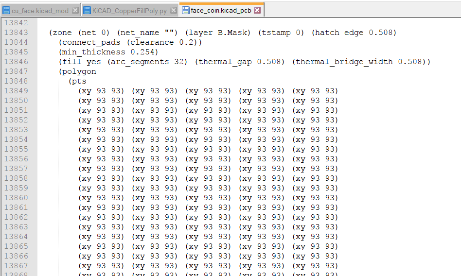
I wanted to put my personal details on the back of the PCB to create a one-of-a-kind business card. Simple, right? A bit of silkscreen text, and job-done! Ah, damn, no soldermask, means no silkscreen is going to stick to the FR4. So I need a circle soldermask layer for the bottom to match the size of my board. Unfortunately, creating a zone with that same circle tool is not as easy. For some reason it just doesn't seem possible. Lucky others have found this problem before me. A quick google search gives me this KiCAD forum with a python script ready for making these zones. The python script is attached in the files.
With a few basic modifications to the script, I could create the circle of diameter 50mm, and I even left a little segment bare on the bottom, just because it looked nice in the viewer. (Thinking about it now, I don't think it will look nice in real life with bare FR4, but time will tell).
The steps are:
- Create any zone in the PCBnew project. Save and close.
- Run the python script, output to a file.
- Copy the output of the python script into the kicad_pcb file, overwriting the contents of the zone, but keeping the shell. It should look something like below.
- Save the file, and re-open in PCBnew. Move it into location as desired.
![]()
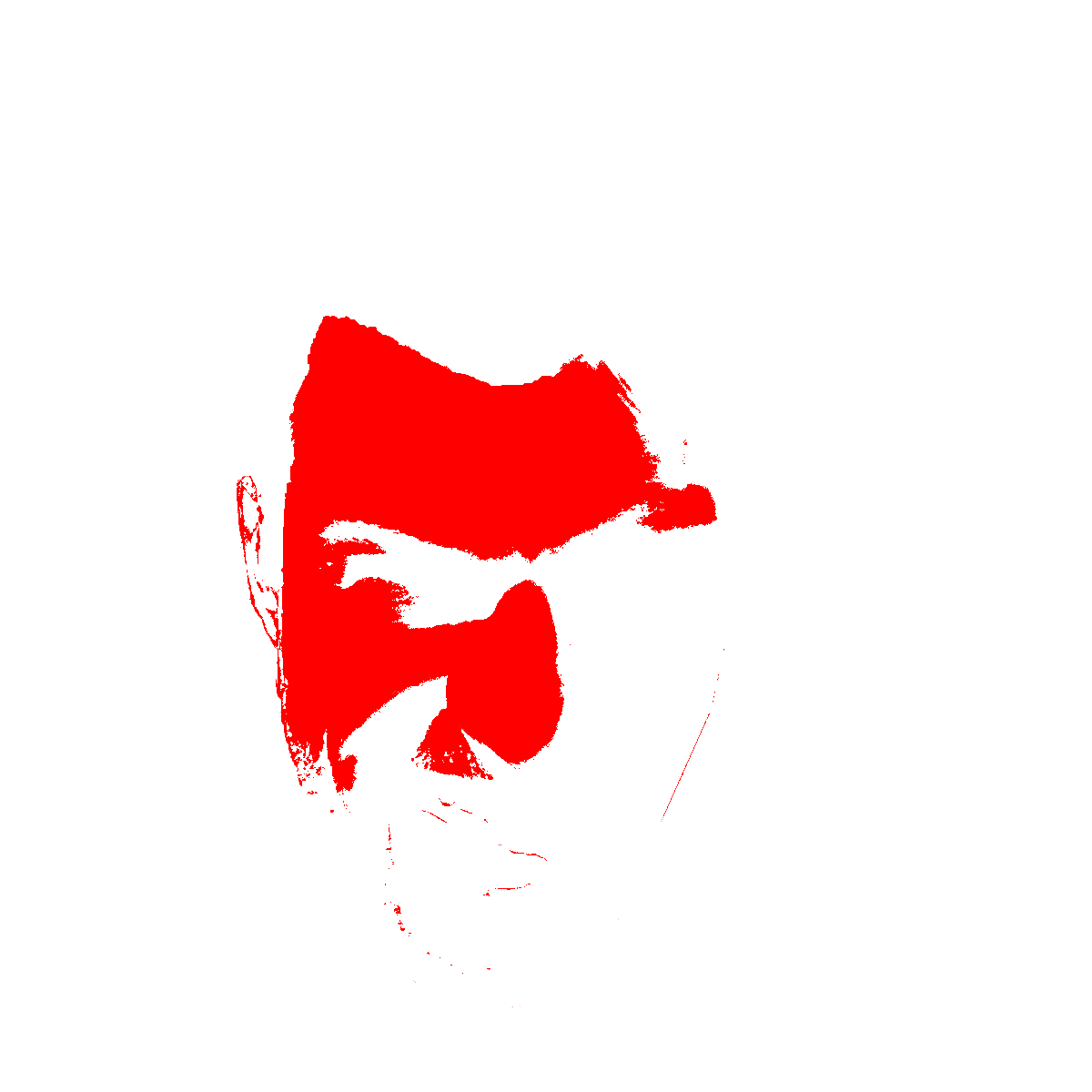
Finally, a few lines of silkscreen later, and I have a design ready for the PCB house. Final images below, with my actual details removed.
![]()
![]()
So the colours will be slightly different than intended, because I am going with DirtyPCBs, rather than OSHPark, but that shouldn't make much difference to the overall concept. I was tempted to order all the different colours to see which was nicest, but decided that it would be better prove that it works first. If the first batch turn out ok, then I will order the remaining 4-5 colours!
I hope to update this with the images of the finished boards when they arrive. (next year)
-
2Step 2: Photo Editing
I'm using GIMP, just because I have used it a few times. It is easy enough to get used to, especially when you can google just about anything you want to do on it.
First, I need to decide which colours can be merged into one. I have 4 colours to work with, as I need 1 for the background. This limits the amount of detail that can be shown in the image. I chose an image with high contrast, and lots of contrast on the facial features. Here is the planned colour scheme.
Num Colour Feature 1 White teeth/highlights in hair 2 gold most facial features 3 beige/brown darker facial features (chin) 4 light purple background 5 dark purple hair/beard/shadows These features can now be split up using the 'scissors select' tool in GIMP and copied to a new layer. I made a single layer for each of the colours, and then used a large paintbrush to paint each layer a single colour. This will help the Bitmap2Component program to separate the layers later.
You can see some of the separated layers below:
![]()
![]()
![]()
This step actually took the longest (probably 4-5 hours). There were a number of iterations before I finally settled on this method. I tried at first to colour each section a different colour and then to export as a single png image. This was quite difficult to separate in bitmap2component, so I changed tack, and created 4 different images for each of the colours (no need to create an image for the bare FR4, because this is a lack of any material).
At the end of this step I now have 4 images:
- cu_face.png
- cu_mask_outline.png
- mask_hair.png
- silk_highlights.png
-
3Step 1: Planning
Planning
Ok, so I want to make my face look like Benchoff. I better go digging through my 10000 selfies! :p Anyway, I found a decent photo, with good lighting contrast. Remember I need to reduce the colour palette to 3 or 4 colours. The photo is included in the attachments. I will use GIMP later to reduce the colours.
Stand on the shoulders of giants. A quick search in your favourite search engine will give a nice list of people who have done something similar before.
- Here is the original Benchoff Buck
- Brian did his own art in KiCad here
- These are really nice lapels, and you could easily see them as cuff-links
All these links provide great inspiration and help for starting out on this project. The main resource that I used was the benchoff buck blog, as it shows a great explanation of how to import the image into KiCad. Because of this, I ended up designing to the OSHPark colour palette that Andrew provides on his blog, even though I have ordered with DirtyPCB. Maybe I will update this later with the actual colours that they turn out.
Num Material Colour PCB layers 1 Silkscreen white Silk + Mask 2 Copper/HASL gold Cu 3 Bare FR4 beige/brown None 4 Soldermask on Copper light purple Cu + Mask 5 Soldermask on FR4 dark purple Mask In KiCAD I need to use the Bitmap2Component program to generate the component layers from the image, and I also need to edit the component manually to fix it up after generation.
Some things to note on Bitmap2Component:
Use the Black & White Picture tab to see what will be generated as a layer in the footprint. The white is the important colour. Rather than using different colours in one png file, I created different 2 tone images with all the parts of the full image. This makes it easier to threshold in Bitmap2Component. I just needed to use the negative or normal setting to get what I wanted.
Also check the size of the image when importing. We have control over the DPI, so to make the imported size smaller, increase the resolution. I aimed for 50 mm x 50 mm because that is the maximum size DirtyPCBs accept on the cheapest run. And also because it needs to be bigger to fit my head!


Discussions
Become a Hackaday.io Member
Create an account to leave a comment. Already have an account? Log In.