 Eric Hertz
sdramThing was recently featured on the Hackaday Blog! Thanks Al Williams!
SDRAM Logic Analyzer Uses An AVR And A Dirty Trick | Hackaday
Note that sdramThing4.5 (this project) has pretty much reached an end. The next phase is more of a peripheral--using these same "dirty tricks"--which can be connected to any uC, SBC, or even a PC's slow parallel port. Check it out at #sdramThingZero - 133MS/s 32-bit Logic Analyzer
(which was also recently-featured on the blog! Thanks Benchoff!)
For an electrically much-simpler circuit to drive an old laptop LCD display using just an AVR and two TTL chips, see: avr-lvds-lcd (it can even be done with an 8-pin ATtiny85 with only 512B of RAM!).
I should also give some credit to this project: http://tinyvga.com/avr-sdram-vga for introducing me to SDRAM's Burst-Mode which sdramThing relies on *heavily*.
This description is quite a bit outdated... I'm at sdramThing4.5, and many of these notes are from 3.0... Beware ;)
What is sdramThing?
This project (sdramThing3.5, now) implements a logic-analyzer interface for an analog oscilloscope.
It works by sampling data at high-speed, then repeating that same data quickly-enough that it can be seen as a bright steady trace on an analog oscilloscope.
Currently, it samples and repeats at 20MS/s. 64MB of a 128MB SDRAM DIMM is dedicated to storing these samples, and it has the ability to sample/repeat 32 bits simultaneously (2MSamples per input). Two of these channels are output as Red and Green on an old laptop display.Cursors are used to select and repeat only the interesting portion of the sample, triggering the oscilloscope at the beginning of the selected-data, then repeating the selected samples several times. This back-to-back repeating of short-duration samples allows for bright traces on a 'scope, even at high "zoom".
This sample/repeat process is made-possible by sdramThing's "Free-Running" mode. This mode takes advantage of the SDRAM's synchronous nature to allow it to control itself. (See below, for more details).
In Progress:
The particular project that inspired this project has requirements outside sdramThing3.0's ability. My data-source appears to have a clock-rate of 25MHz, while sdramThing3.0 has a sample-rate limited to the AVR's clock-speed of 20MHz.
Thus, I've revisited looking into making use of the SDRAM's ability to run at speeds much faster than my AVR (thus: sdramThing3.5).
It's entirely plausible, with a bit of work, to get sampling up to (and exceeding) the SDRAM's rated clock-speed of 133MHz (133MS/s). But currently, I'll be happy to get it working at 40MS/s, as my attempts at decoupling the SDRAM clock from the AVR clock have been slow-in-progress.
The current status, as has been for a while: I have designed and soldered-up the "one-shot" circuitry necessary for decoupling the clocks, but, ironically, it's not even working with that circuitry in "bypass" mode. I've been fighting this for a while, now. Finally, I've reimplemented the ability for the AVR to read-back the data it wrote to the SDRAM, so maybe I'll get somewhere soon :)
Details (a tiny bit outdated):
For more info on Free-Running SDRAM and sdramThing3.0, click here.
As I'm refreshing my memory on how it works, so as to fix some bugs and improve functionality, I'll probably throw some relevant notes here, both for you and for me ;)
sdramThing3.0 makes use of two groups of memory on a typical DIMM. The "Free-Runner's" memory is loaded with all the commands which are fed back to both devices' command/address-inputs. Thus, the SDRAM actually sends commands to itself, and runs "free" from (independent of) external control (like the AVR).
The "Side-Kick" has two modes: Write and Read, which correspond to the "logic analyzer's" Sample and Repeat.
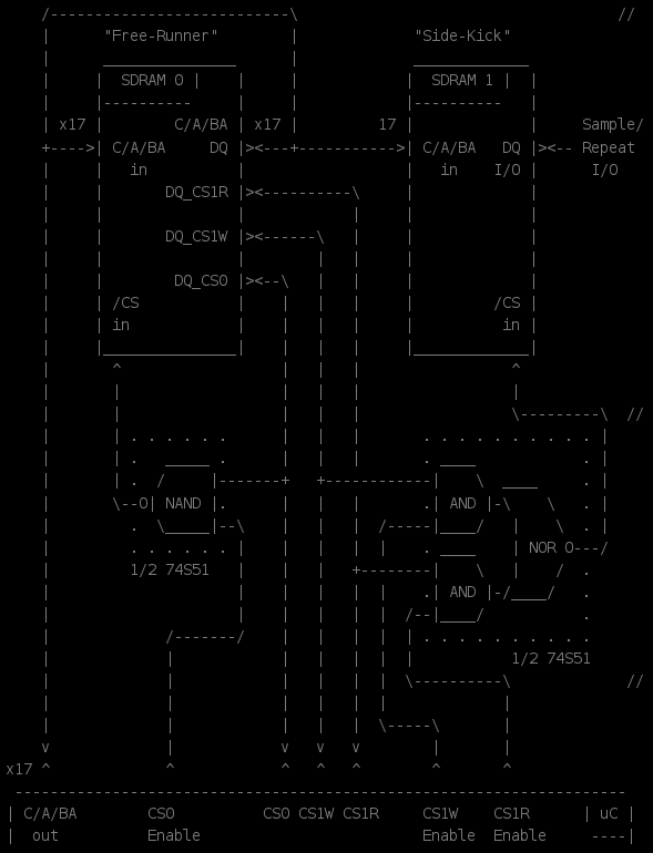
Multiplexing-logic allows for selecting the mode... The Free-Runner is loaded with commands for both Read and Write for the Side-Kick. Both commands are always output. The logic enables the read commands for repeat-mode, and enables the write commands for sample-mode. Thus, the MCU need only toggle the appropriate Enable pin, as necessary, no more than once per *entire* load/repeat of the SDRAM. The Free-Runner takes care of all commands and timing for continuously cycling through the individual pages in memory.
For now, there are three different sorts of fed-back/free-running commands:- Commands that are fed to both the Free-Runner and the Side-Kick, regardless of the mode (Sample vs. Repeat). These include Precharge and Activate, which are used to close a previous page and open a new one.
- Commands that are sent to the free-runner every time, but only to the Side-Kick when it's in "Repeat" mode. These are the "READ" commands, which actually begin a new read-burst at the next page.
- Commands that are only sent to the side-kick when in "Sample" mode. These are the "WRITE" commands, which begins a write-burst in the next page of the side-kick.
//   Page 0:                                Page 1:
// ---------------------------------      ---------------------------------
//| ...| P_FS | A_FS | R_FSr | W_Ss |--->| ...| P_FS | A_FS | R_FSr | W_Ss |--> ...
// ---------------------------------      ---------------------------------
Where:- P_FS = Precharge Free-Runner AND Side-Kick
- (Close the next bank, which is still open at the *last* row, so it can be reopened at the next row)
- A_FS = Activate Free-Runner AND Side-Kick
- (Open the next bank at the next row)
- R_FSr = Read Free-Runner AND (Side-Kick when in "Repeat" mode)
- (Issue a Read at the next bank, it will occur a bit later due to the CAS Latency)
- W_Ss = Write Side-Kick when in "Sample" mode.
- (Issue a Write at the next bank)
(Note that because of the Read CAS-Latency, the Read and Write commands, despite being offset in memory, point to the same column in the same (next) page at the same time. Handy!)
This pinout is slightly outdated, sdramThing3.5 has replaced Tx0 on PD6 with the "oneShotEnable" pin. When "oneShotEnable" is disabled, the one-shot circuitry is placed in bypass mode. It *should*, then, function identically to sdramThing3.0... but it's not yet there. (UPDATE 3-4-15! It now works in bypass mode! One-shot is coming soon!)
This pinout is for sdramThing3.0.
//                             ATmega8515
//                            ____________________
//                           |         |_|        |
//                SDR_nWE  --|  1 PB0      VCC 40 |--  +3.3V
//               SDR_nCAS  --|  2 PB1      PA0 39 |--  SDR_BA0
// (AIN0)        SDR_nRAS  --|  3 PB2      PA1 38 |--  SDR_BA1
// (AIN1)         SDR_CS0  --|  4 PB3      PA2 37 |--  SDR_A0
//               SDR_CS1R  --|  5 PB4      PA3 36 |--  SDR_A1
// (PGM_MOSI)    SDR_CS1W  --|  6 PB5      PA4 35 |--  SDR_A2
// (PGM_MISO) +-/\/\/\-|>|---|  7 PB6      PA5 34 |--  SDR_A3
//  (PGM_SCK)     SDR_CKE  --|  8 PB7      PA6 33 |--  SDR_A4
//              (PGM_RST)  --|  9 /RST     PA7 32 |--  SDR_A5
//  LCD_R               /  --| 10 PD0      PE0 31 |--  SDR_CS0_En
//  LCD_G              |   --| 11 PD1      PE1 30 |--  SDR_CS1R_En
//  LCD_DVHB SDRAM     |   --| 12 PD2      PE2 29 |--  SDR_CS1W_En+TrigOut
//  LCD_CLK  Data     <    --| 13 PD3      PC7 28 |--  SDR_DATA_DQM
//                     |   --| 14 PD4      PC6 27 |--  SDR_ADDRCMD_DQM
//                      \  --| 15 PD5      PC5 26 |--  SDR_A11
//                 Tx0     --| 16 PD6      PC4 25 |--  SDR_A10
//  anaButtons In ----+------| 17 PD7      PC3 24 |--  SDR_A9
//                    |    --| 18 XTAL2    PC2 23 |--  SDR_A8
//                   ---   --| 19 XTAL1    PC1 22 |--  SDR_A7
//                   ---   --| 20 GND      PC0 21 |--  SDR_A6
//                    |      |____________________|
//                    V
//
// Scope Trigger Output is connected to PE2, multiplexed with CS1W_En
// (risky? Isn't there a better choice?)
//
// LCD_R and LCD_G are connected to two of the "Side-Kick's" DQ pins
// LCD_DVHB and LCD_CLK are connected to two otherwise-unused "Free-Runner"
//   DQ pins so that the LCD timing information won't be overwritten when
//   sampling
Data-Masks.
The SDRAM's data-mask pins (DQMs) are used to enable reading *and* writing of data via the DQs (Data I/O pins).
Note, first, that Read/Write commands are *burst-oriented*, so sending a "read" command to address 0 means that after a slight delay the data at address 0 will be output, then address 1, then 2, and so-on until address 1023. Similarly for "write" commands.
When Reading: If the selected DQM pin is high for a clock-cycle, the corresponding data, which would arrive a clock-cycle or two later, is *not* output. OK, this makes sense. It's basically an output-enable (but since the chips are Synchronous, it's slightly delayed).
When Writing: If the selected DQM pin is high for a clock-cycle, then the data driving the DQ pins during that clock-cycle is *not* written to that location in memory... In this way, it's possible to run a "write-burst" and only end up writing to *one* location in that burst.
sdramThing3.0 uses this to its advantage... Note that the "C/A/BA" pins (Command/Address/Bank-Address) are wired directly to the same SDRAM chip's Data pins.
For the AVR to write data to the "Free-Runner" SDRAM chip(s):
Mask the SDRAM chips' data I/O pins that are wired to its C/A/BA pins (set the appropriate DQMs high)
Load the "write" command and address to the AVR's C/A/BA outputs
Strobe CS0
Load the data to be written into the SDRAM to the AVR's C/A/BA outputs
Strobe the DQM low for a single clock cycle
Normally, a "write" command would write data at the selected address during that same clock-cycle, then continue to write the consecutive addresses from there-on.
Instead, we're telling it *not* to write data *until* the DQM is strobed... So the "Write" *procedure* is started, but no writing occurs while we set data-values on three separate ports (requiring several clock cycles). Once those port-values are set, *then* we strobe DQM to write to a single memory-location (using burst-mode).
This requires a bit of planning, and actually I'm using assembly for the actual procedure listed above. E.G. if it takes 5 clock cycles between the strobing of CS0 and the strobing of the DQM, then that needs to be accounted-for in the address. If I want to write at address=100, I have to subtract 5 from that and send a "Write-burst" command to the SDRAM starting at address 100-5=95.
The write-burst then starts at address 95, but data is only written to address 100, when the DQM pin is strobed.
Similar can be done for reading.
(In Free-Running Sample/Repeat modes, the DQMs are inactive; all data I/O is enabled during Free-Running. Thus, the AVR has direct-control over the DQMs at all times, but the DQMs needn't be toggled except when the AVR is reading/writing the SDRAM.)
In The Works: sdramThing3.5 Full-Speed:
I've discovered that even 20MS/s isn't fast enough for spying on the motor-driver's data. I think it's transmitting closer to 25MHz.
I've had plans in the works, since the very beginning (sdramThing1.0) to try to run the SDRAM at its full-speed (133MHz=133MS/s).
Doing-so has been put on the back-burner for a while, but now I'm thinking about it again... sdramThing1.0 may have lent itself better to one-shot circuitry, as it didn't require the precision-timing of the DQM-strobing method described above.
The idea is to use one-shot circuitry running at the SDRAM's clock-speed, driven by the AVR's outputs. I *think* all that needs to be one-shotted is the Chip-Selects and DQMs. (Looking into full-speed/one-shot is why I came across the need to remind myself how the DQMs are implemented).
So, then, if the processor is running at 10MHz and the SDRAM is running at 100MHz, then every processor cycle would correspond to 10 SDRAM cycles... The one-shot circuit would look for the appropriate edge on the appropriate pin (CS/DQM), output that value, then immediately deactivate it after *one* SDRAM clock (even though the AVR's outputs still show it as active). So the DQM-strobing method, described above, would occur 50 address-locations after the CS-strobe. I think it's possible, but, again, it's been a while since I really understood how this whole system worked. Also, as I recall, sdramThing3.0 didn't really take the future-plans for one-shot circuitry into account (that idea was looked into quite a bit during the sdramThing1.0-era).
sdramThing3.5 is in the works. The one-shot circuitry has been designed and soldered. But currently only functions in "bypass" mode, which is software-wise identical to sdramThing3.0. This new circuitry sits between the AVR and SDRAM on only the DQM and Chip-Select Enable pins.
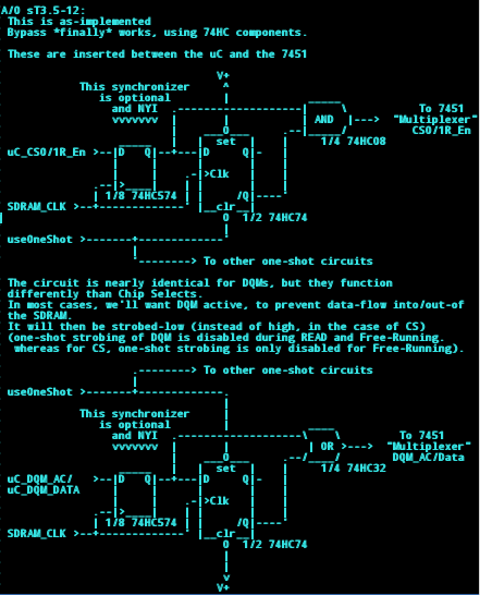
(I'd originally planned on using only '574s, but that 7474 removed *several* gates. Nice.
UPDATE 3-14-15:
Moving on to sdramThing4.0, now... Really, 3.5 shoulda been called 4, but I guess it was an intermediate step.
This is still intermediate, but the wiring has changed, again, only slightly.
The one-shots apparently aren't quite functional. They allow two bytes to be written consecutively with the same value. Somewhere in the clocking system and gate-delays (?) there appears to be an output that's active during two positive clock-edges... I'm guessing *right before the beginning* of one, and *right after the end* of the other (thus, it's only slightly wider than one clock-width).
The fix... for now... Since it writes each value to two consecutive columns and I don't use the last two columns in each page, it's OK this occurs *as long as* each write happens consecutively (overwriting the bogus data with correct data, everywhere except the unused column(s) at the end).
So... I tested it, and it almost seems to work. Except one glitch. Writing the Blue data (the cursors and status-bar) does not occur consecutively. A pixel may be written here or there, and the remainder of the page won't be rewritten. Thus, after each blue pixel-change, there's likely to be a column of invalid data. Quite likely this invalid data will occur at a Free-Running command.
So. The Fix (and, really, I'd considered doing this before anyhow):
Put the Blue data on a different SDRAM chip altogether. Pretty simple, really... and the nice thing about a DIMM is it's chalk-full of chips.
So, yeah, as long as this glitch isn't fixed, the blue pixels will likely be double-wide. But that doesn't really matter.
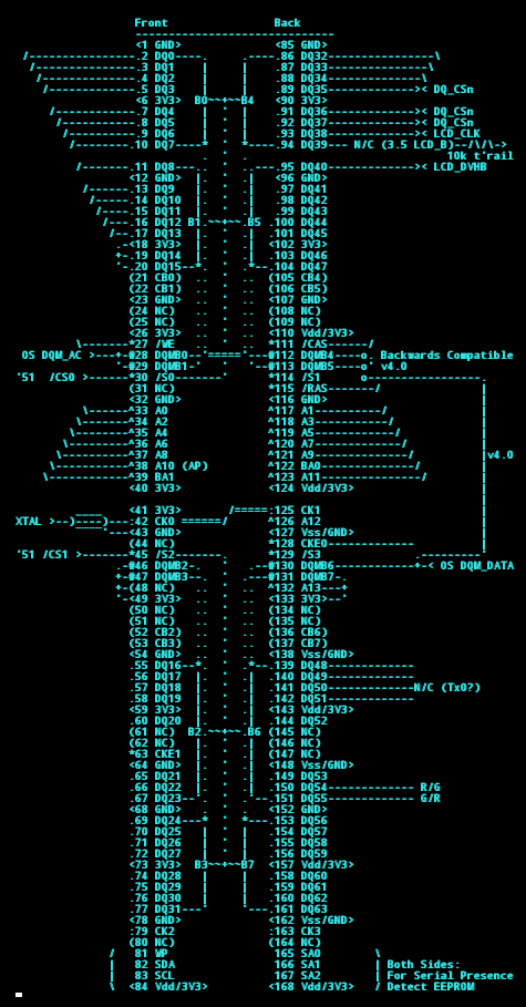
Below is the pinout of the SDRAM DIMM, and a bit of my wiring-scheme...
Note the change to pin 94, it once held LCD_DVHB (That's Data-Enable, V-Sync, H-Sync, and Blue).
That was on the same data-byte/chip as Free-Running commands.
Now, it's been relocated to pin 95, which is on a separate byte/chip.
The same *commands* are written to all chips in that group (/S0) (The "Free-Runner"), but the DQM has been separated. DQMB5 can now be connected, via jumper, to DQM_AC (which is shared with DQMB0, 1, and 4 for free-running) in order to run identically to the old configuration (for compatibility with old software). Or, it can be jumpered to DQM_DATA, to make it 4.0-compatible.
The other key-factor, here, is that blue-data is only written on the screen (as opposed to during the LCD's blanking-periods). Thus, the Data-Enable, V-Sync, and H-Sync bits remain constant, and shouldn't....
dammit.
No.
This data is stored *serially*, of course.
... So. I guess I might be able to take advantage of the fact that the V-Sync and H-Sync signals are both inactive... write each pixel all the way up to V-Sync, and allow it to overwrite H-Sync.
Oy.
YES. In the Long-Run, I do plan on fixing these one-shots. This was supposed to be an easy work-around ;)
(And a details-update rather than a project-log, sheesh)...
Anyhow, reasonable progress toward the betterment of the project, anyhow.
Some more code has been cleaned-up and better-documented.
I did, kinda, always want to have that 4th byte/chip on the Free-Runner available for specialized-purposes like these. It always outputs along with the Free-Runner (so can't be used for sampling data), but could be useful for data that changes (like the blue/cursor data). Possibly, also, things like a trigger-output (which would move depending on the cursor-position), etc.
Previously, changing this sort of data meant rewriting the Free-Running data, as well. Easy enough, the function was already written to handle it all simultaneously, but it does require a bit of unnecessary recalculation. Maybe I can speed-up those cursor-movements ;)
Another purpose, it's similar to sdramThing1.0(?) which had a smaller (in MB) SDRAM... so in order to free-run an entire LCD-frame required switching the DQM halfway-through, swapping which chips are used between the upper-half and lower-half. In that way, I suppose, Free-running could be doubled-in-length (doesn't help the LCD, but would plausibly be useful for *longer* samples... MAYBE it's plausible to cause the LCD to scroll with the cursors...).
Anyways, it wasn't exactly the path I was planning to take from the start, but it hasn't been un/counter-productive.
And, I finally have a friggin' pinout for the SDRAM DIMM. It's about time. It was all *notes* before, never a drawing... It didn't make sense to me why chips 0,1,2,3 corresponded to bytes 0,1,4,5 until seeing it 'graphically'.