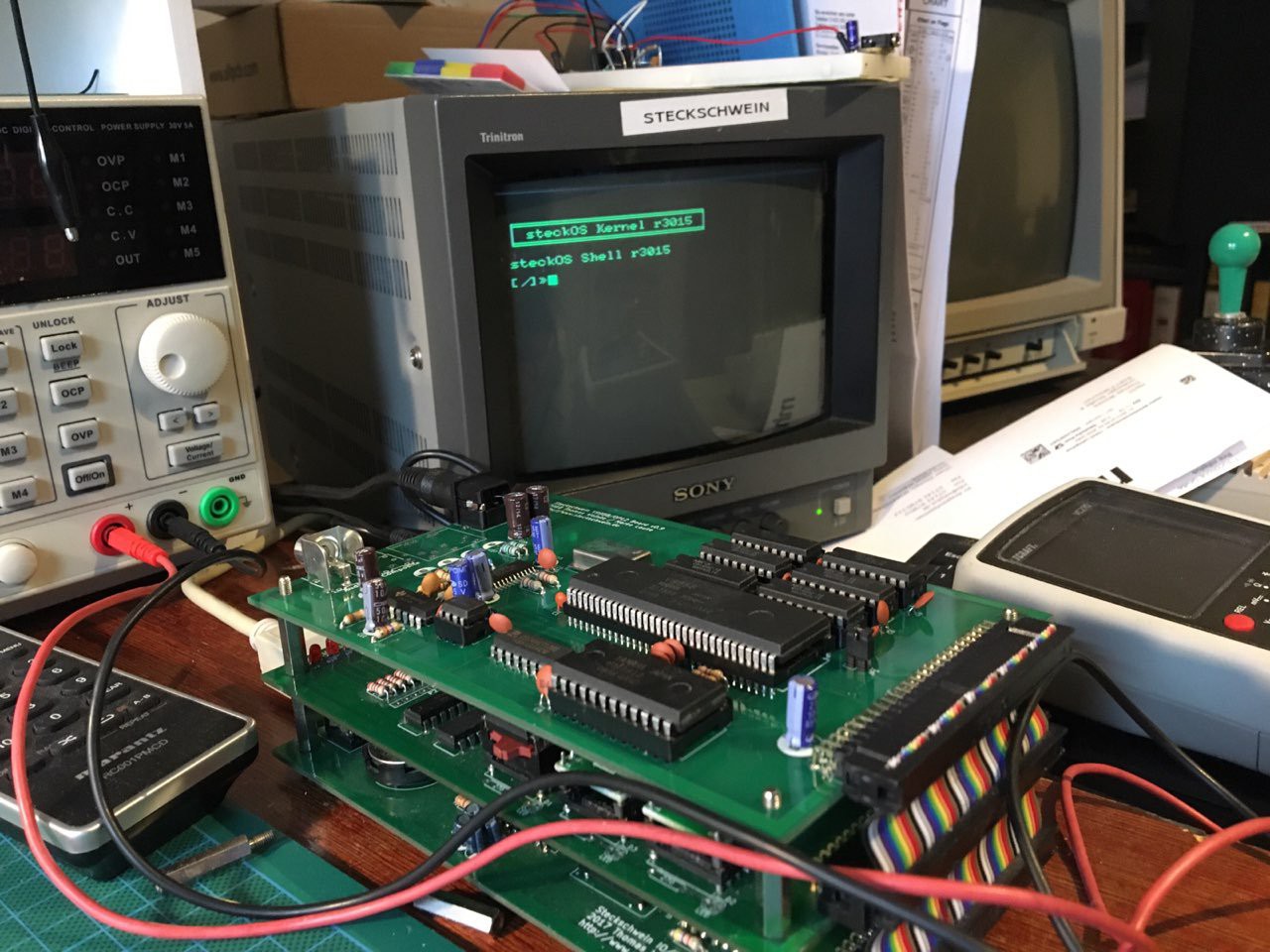
Having evolved from the breadboard stadium a while ago, the Steckschwein is divided into 4 main units, each located on a separate circuit board. The boards are connected through a piece of 50pin flat cable, not unlike a SCSI II cable, but much shorter. The main units are:
- CPU/Memory board
- I/O board
- Video board
- Sound board
This approach allows us to upgrade one of the units without having to design a whole new pcb. Our main goal however is a single board version of the Steckschwein.
The current specifications are:
- 65c02-CPU running at 8MHz
- 64k RAM
- 32k ROM
- Video chip V9958
- Sound chip YM3812 (OPL2)
- rs232 via UART 16550
The following sections will describe the main units in more detail.
CPU/Memory board
This is the heart of the Steckschwein computer (obviously) and consists of the 65c02 CPU, 64k RAM divided into 2 32kx8 SRAM chips, 32k ROM on a 28c256 EEPROM, divided into banks of 8k, and 2 GALs for address decoding and wait state generation. The memory map is as follows:
| Adress | Description |
|---|---|
| $0000-$00ff | Zero Page |
| $0100-$01ff | Stack |
| $0200-$02ff | I/O area |
| $0300-$7fff | RAM |
| $8000-$dfff | RAM |
| $e000-$ffff | ROM/RAM |
We put the I/O area just behind the stack to get the most possible amount of unfragmented RAM. Also, the address decoder is capable of mapping out the ROM entirely. Any writes to the ROM while it is mapped in will go to the underlying RAM. Yes, this has been heavily inspired by the C64.
We actually make use of this when booting SteckOS. The "OS loader" will write the kernel "under" the ROM, then map out the ROM and jump to the kernel init routine. Also, this proved to come in very handy when testing new BIOS versions before finally burning them to EEPROM.
I/O board
The I/O board is where the Steckschwein talks to the world. A 65c22 VIA's port B is used as a SPI master (semi bitbanged), port A is used for the joystick ports and also doubles as user port. In it's latest incarnation, the I/O board also contains the 16c550 UART, which had it's own board before.
We use SPI as the main peripheral bus because it allows us to use SD cards as storage device. That way, we get gigabytes of storages for almost no hardware effort. Theres no reason do deal with disk drive controllers in 2014. Also, we use a ATmega8 micro controller to interface between a PS/2 keyboard and SPI. The last SPI device is a Maxim DS1306 real time clock, which also has a nice feature of 96 bytes of battery buffered memory, which we use to store a few parameters (boot file name, uart baud rate, etc.)
Video board
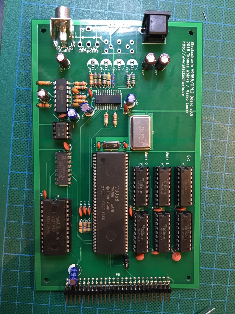
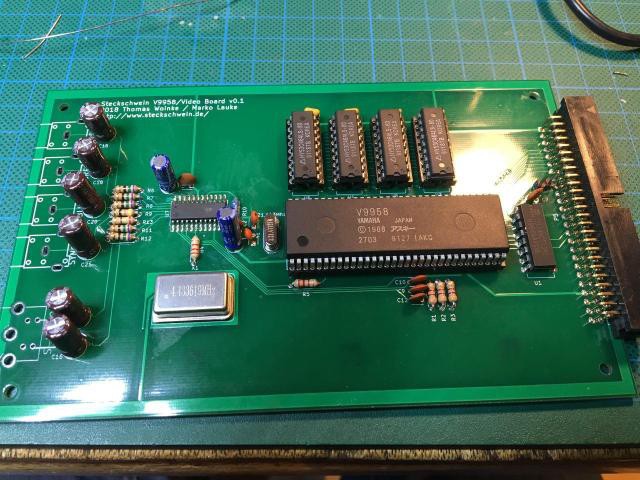
We now use a V9958 VDP, the TMS9929's successors successor with 128k DRAM. This chip does not generate YpBpPr, but RGB video. We use a CXA2075M as output stage and for generation of compsite video and s-video.
Old Video board
One thing about the TMS9929 video display controller compared to it's US sibling TMS9918 is the output of YPbPr video, which made it necessary to put a converter circuit tp RGB on to the board, too. Also, it only supports 4116 or 4164 DRAMs natively. DRAM proved to be a real pain on a breadboard (our experiments with the 9929 and DRAMs eventually led to the decision to finally design PCBs), especially those 4116 things which need 3 operation voltages (-5V, +5V and 12V). Also, those old DRAM chips are increasingly hard to come by, so we went with an alternative circuit which allowed us to use another 32kx 8 SRAM.

 Keith
Keith
 fjkraan
 Colin Maykish
 Stephen Moody