 fjkraan
The Oval UD-80 Display Controller is based on a CP/M feature to redirect input and/or output, typically configured with STAT (see Fun with STAT).
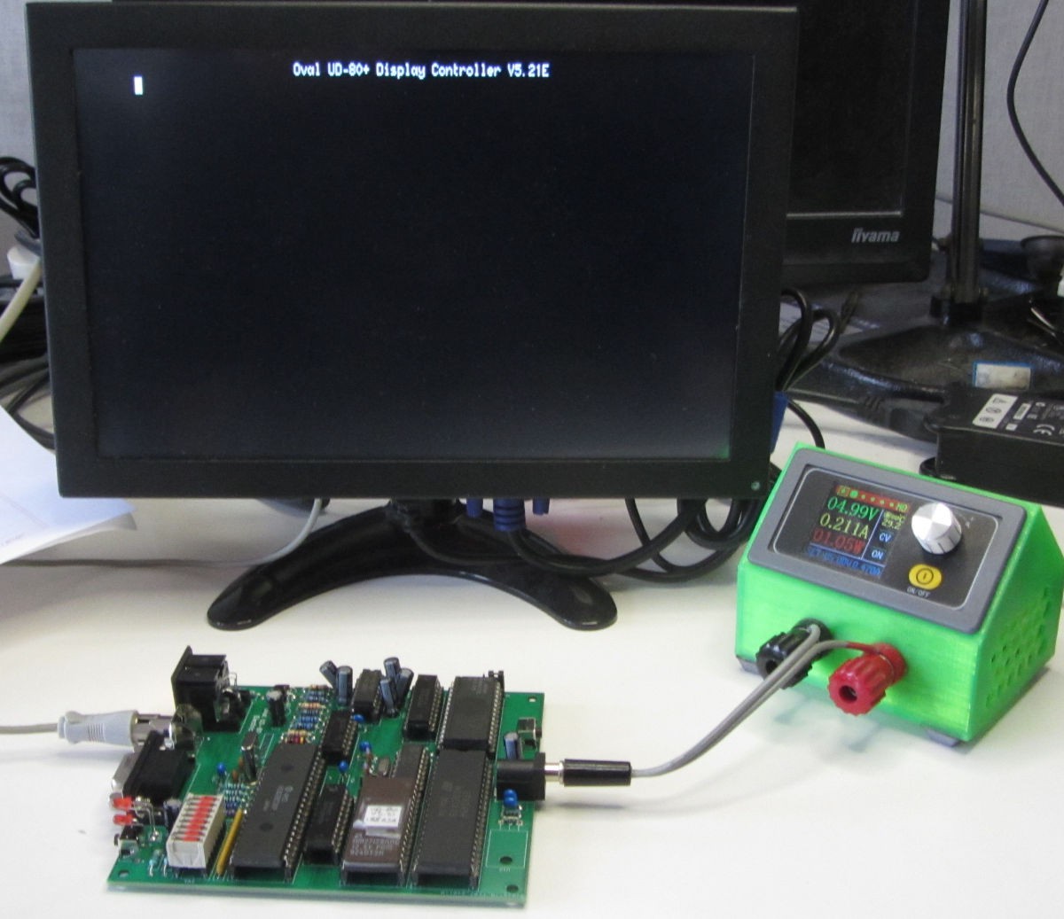
The UD-80 displays the output (80*24 or 40*24) on a cheap TV compatible monitor (PAL or NTSC). Very sensible in the 1980's. The driver allows to add color information, but lacking the original manual it is unclear how.
The driver isn't compatible with the old OS-ROM (M25030CA), and it instead suggests the STAT option.
For the PX-4 more testing is needed, but the STAT command below works.
STAT CON:=TTY:
Here a review of the device from 1986:
Epson Connect review of the Oval UD-80 (198603)
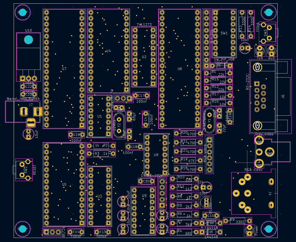
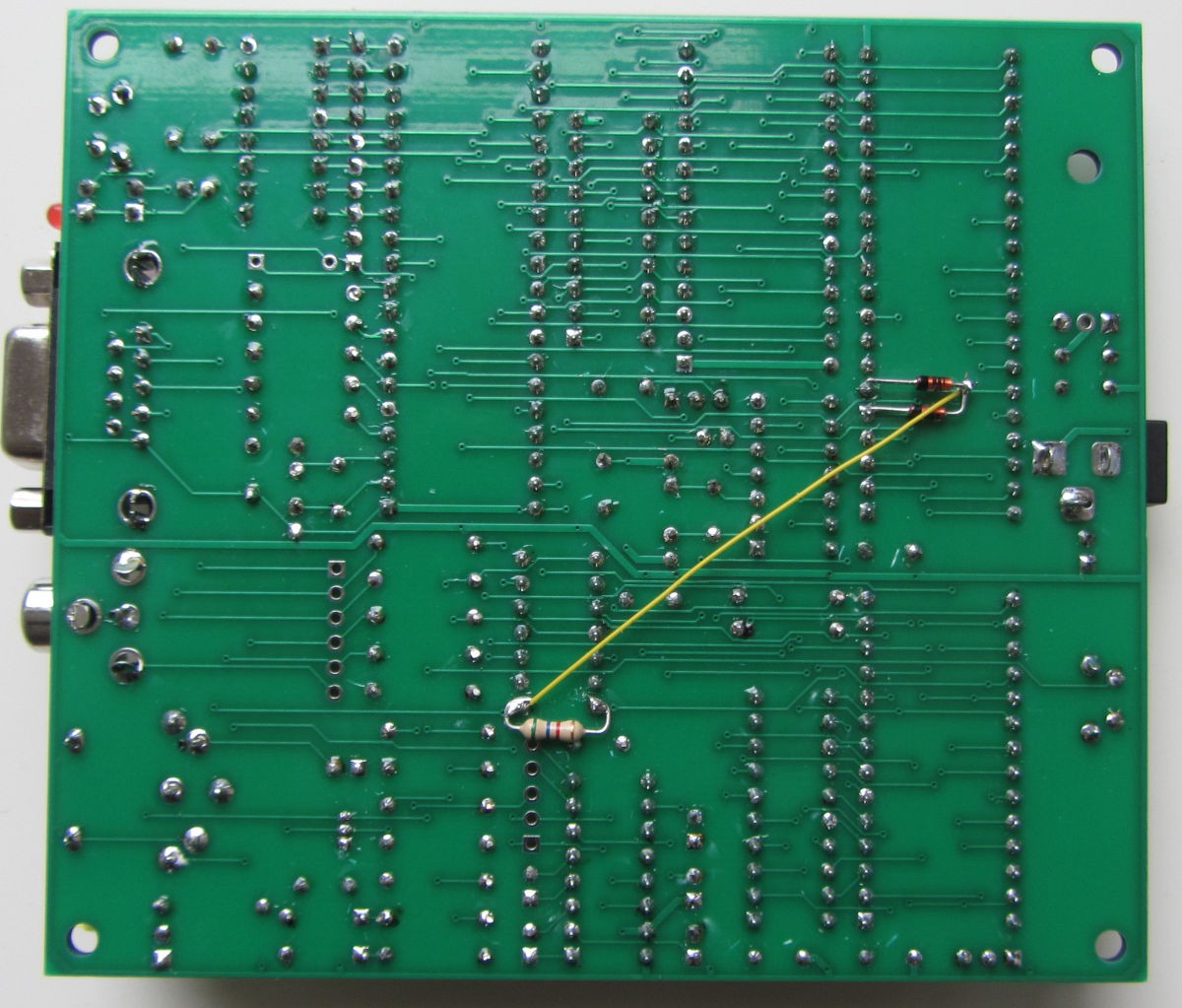
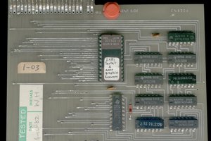
There are two different firmwares available; 5.21E with a driver for the PX-8, and the patched 7.11c with a driver for the PX-4. Both firmwares probably work with both machines. The original 7.11A firmware does not work with the standard UD-80 and the Re-UD-80, as this firmware expects lightly different hardware (see the log on "The sync issue and two firmwares").

 Keith
Keith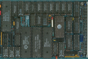
 Plasmode
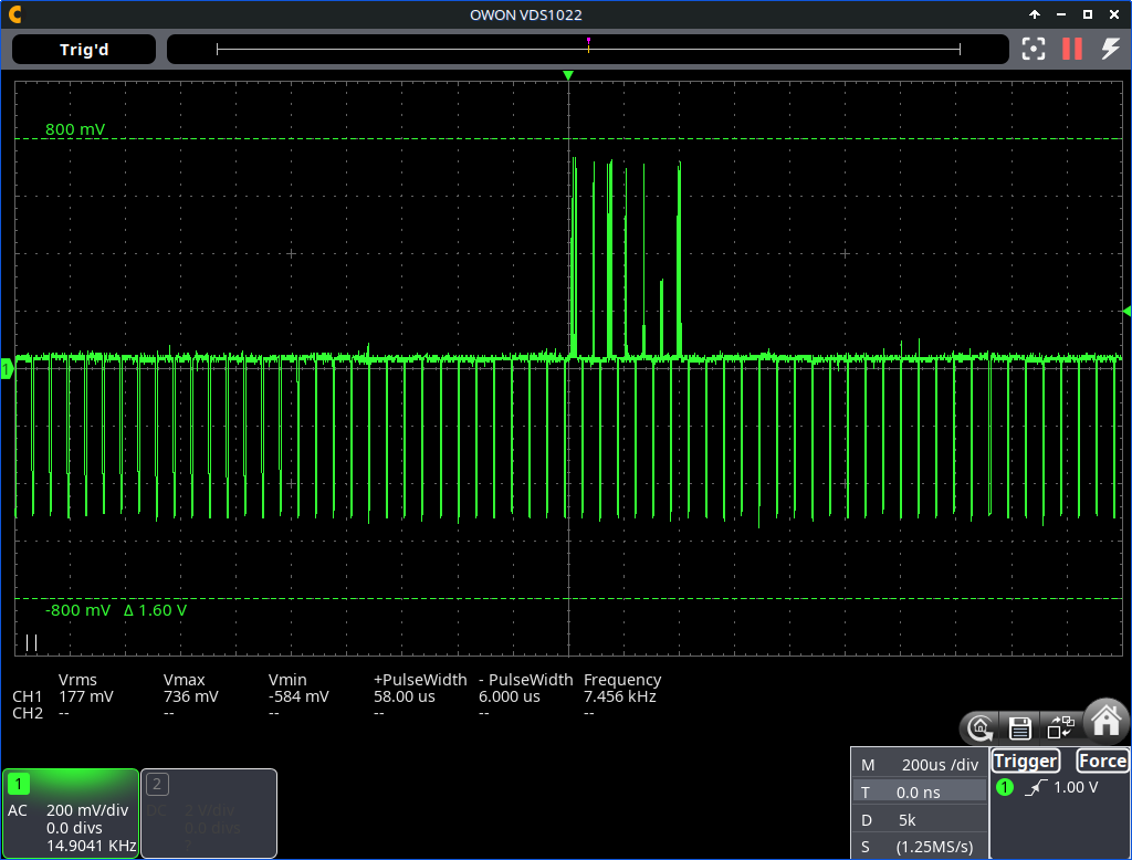
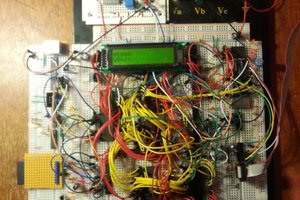
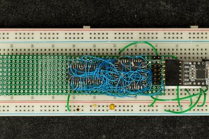
The simplest way of testing if the HX-20 will work with this device is connect the HX-20 to a serial port on the PC (4800Bd, 8bits, no parity, 2 stop bits) and type 'SCREEN 1, 0'. If this works, the Re-UD-80 will work too.