Close
0%
0%

Little PLC

A small but versatile PLCish craddle for an LPC1769

Similar projects worth following
I needed to read a couple of sensors and send the information over RS-485. Since I had a couple of LPCpresso1769 boards laying around I decided to use them. The LPC1769 is quite the uC and was kind of an overkill for this so instead of using another microcontroller I decided to increase the capabilities of the device.
I ended up with what you can see on the pictures.
So far it has:
Inputs:
4 analog inputs, 4-20mA or 0-10V selectable individually by jumpers
8 optocoupled inputs
Outputs
4 open-drain mosfets
4 relays
1 analog output, 4-20mA or 0-10V selectable by jumpers

Comunication
1 RS-485
1 CAN
1 Ethernet
1 USB device
Memory
1 64K I2C (included in the LPCxpresso)
Power Supply
+24V (used a simple switching power supply @150khz)

So, as I said, I needed to get information from a couple of sensors a send it over RS-485. This was for a project that needed to monitor pressure and volume of fluids injected to an oil well. The information would then be displayed on an HMI (human machine interface) with a 10" screen that we're developing around an OlinuxinoA20 board.

There were to paths to follow. I could build the hardware just for what I needed or I could go the extra mile and build something that could be useful for future projects. Needless to say I followed the second.

Around this time I was paying close attention to the CIAA (not CIA) which would translate to something like "Open Source Argentine Industrial Computer" which is an open source PLC. It comes in many uC flavors and you can get everything you need from their website. I've never worked with a PLC so I took this design as a reference to get an idea of which IOs would be useful to include as well as communication protocols, power supply voltage, etc.

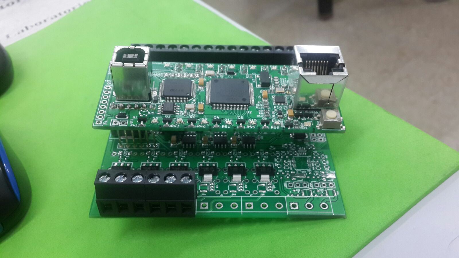
On the other hand I was used to working with NXP family of ARM uCs. The LPC1769 in particular always seemed quite powerfull and feature rich so I picked it right away. Luckily it had every interface I needed, even D/A! which is not that common. At this stage of the design I didn't want to be bothered with designing the PCB that would hold this IC. Mainly because the first batch of PCB were going to be homemade and since I'm not yet able to produce PTH, the routing would get quite messy. So instead I decided to take advantage of the LPCXpresso board and just make a craddle for it. By doing this I could get the IC routed and soldered as well as the PHY for ethernet and a little I2C memory. This ended up providing two key advantages. The PCB would be much simpler since there were less high-connection-density ICs on the board and I would get a more generic and "uC independent" design. This means that if I want to switch to a bigger processor capable of running Linux I just have to design that board so as to fit in this "PLC motherboard".

The features I have right now implemented can be seen in the following image

I chose this format for the PCB to fit it on a standard case for din rail like this one

I'm gonna have cut a couple of square holes for the ethernet and usb connectors.

So far I'm pretty happy with the outcome although I feel like I should've in included a couple of things more like a micro-sd socket and a pin header with unused uarts, spi, I2C.

The micro-sd would be great to use this as a datalogger but I guess I'll include that in the next iteration. The pin header connector would be useful if I could place it on the edge of the board. This way I could connect other modules just by placing them next to each other. The modules that I'd like to have, and can think of right now, are more IOs, more relays, GPRS, WiFi, etc.

I'll be documenting the project and uploading more of it in the future but in the meantime make sure to check out CIAA's homepage and GitHub! It's an awesome project!

Hope you like it!

  • Been busy with this

    federicoortiz1201/01/2016 at 16:35 0 comments

    So it's been a while since I've written something here. Luckily for me, this project landed me a part time job designing something quite similar with two other guys and a team leader.

    Here are the results

    It has similar functionalities as the one I first published here. It's just tailored to the needs of the customer. Sadly this is a private project so I can´t share the design files.

    On the bright side, I learned how to use KiCAD! This means the next iteration of the project will be completely open source!! (the previous one was design in Altium)

    Here are some more pictures

    As you can see in the pictures, there are some components missing. That's because you can build two different versions of PLC with the same PCB. For example in this case, if you don't place the 6 MOSFETs in the picture you can place 6 relays. Also next to them you can see the unpopulated DAC area that provides 4-20mA or 0-10V output.

    I've learned very much with this project. On the next iteration I would like to set the bases for a modular design that would allow me to connect modules next to the "Little PLC" such as Wifi module, GPRS, IOs expansions, etc.

    If you have any ideas or recommendations feel free to comment!

    Thanks for taking the time to read my nonsense an happy new year!!

View project log

Enjoy this project?

Share

Discussions

Burak Enez wrote 08/14/2016 at 15:16 point

Hi, i also wonder the 4-20mA analog input part. Please can you send me the schematic of this part? email:(burakenez  @  gmail.com) without spaces.

  Are you sure? yes | no

PointyOintment wrote 02/23/2015 at 12:48 point

66

Mainly because the first batch of PCB were going to be homemade and since I'm not yet able to produce PTH, the routing would get quite messy.

99

It took me quite a while to figure out that this sentence is code for "I don't have a PCB drill, so I can't make vias, so I can only make single-sided boards." (Is that the correct interpretation?) That must mean those are SMD terminal blocks… interesting… I've never seen those.

  Are you sure? yes | no

federicoortiz12 wrote 02/23/2015 at 14:52 point

Actually no, this PCB is dual layer. The thing is that vias made with wire can't be placed beneath a component. Usually when you're dealing with a QFP you may end up placing vias under the component. Since actual PTH vias are low profile that's not a problem, here it would've been since the solder of a wire is quite high.

  Are you sure? yes | no

hipernik wrote 02/22/2015 at 06:28 point

Hi, how you can select

4 analog inputs, 4-20mA or 0-10V 

using a jumper, please can you send me a schematic (hipernik     @   libero.it) remove the spaces on the email address

Are you Italian? i'm from Gallarate 

Best Regards

  Are you sure? yes | no

federicoortiz12 wrote 02/22/2015 at 13:45 point

Hi hipernik!

I'll send you the schematic and post an explanation.

I'm from Argentina actually, Buenos Aires

  Are you sure? yes | no

Similar Projects

Does this project spark your interest?

Become a member to follow this project and never miss any updates