 zaphod
As the title suggests this project is not actually dead in the water. My last update was just after the project was exhibited at Maker Faire, when I wrote that update the ROM was ~75% functional. Since then I have completed soldering the 128 diodes needed to bring the ROM up to functionality. The ROM board is now 100% complete, here's a couple of photos:
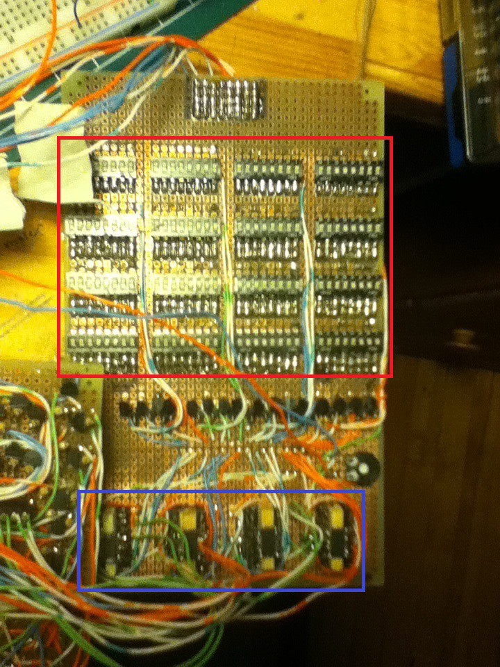
This is the top of the ROM board. The red box shows the actual physical memory. The ROM isn't some semi-abstract thing deep inside of the computer made up of magnetized spinning metal, but rather 128 individual toggle switches. The blue box shows where I ended up using LM339 comparators to clean up the ROM access logic. You can read about that wonderful series of mistakes here.
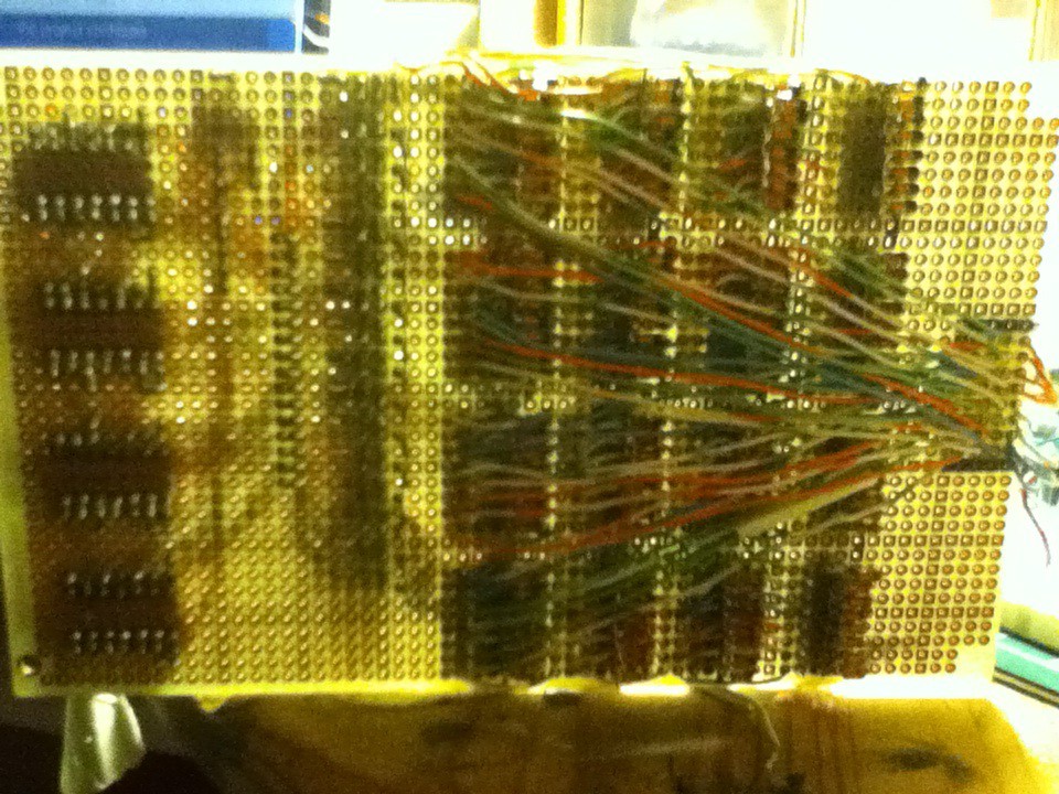
This picture shows the bottom of the completed ROM board on the left hand side of the image you can see the bus lines that feed into the switch banks, and if you look closely you can just make out the diodes I soldered on after the initial construction of the board. The completely new and unique series of mistakes that lead to the diodes can be read about in the link above. Anyway the mess of missteps that I made in the construction of the ROM is now over and the ROM works. To demo the completed ROM I connected the output of the program counter/multiplexer unit to the addressing lines of the ROM and the output bus of the ROM to 8 LEDs. I then toggled the following binary values into the memory:
00000001 // each line represents a memory address
00000010
00000100
00001000
00010000
00100000
01000000
10000000
10000000
01000000
00100000
00010000
00001000
00000100
00000010
00000001
When I hooked up a clock signal I effectively had a crude Larson scanner, which I made a .gif of but is too big to upload :(Now that I have a the ROM complete I'm ready to move onto the next stage of the project. the next piece to build is the instruction decoding logic. this will essentially be another 1:16 demultiplexer with it's input held high. The mux's address lines will be connected to the upper four bits (5-8) of the bus coming out of the ROM. the other four ROM lines will be a binary value to be operated on. however it isn't that easy. because I used comparators to clean up the ROM address signals I need another multiplexer. The comparator's reference voltage is set by a pot on the ROM board. Depending on various factors the pot need to be trimmed to ensure that multiple addresses aren't pushed to the data bus at the same time. The only way to ensure that two addresses aren't superimposed on top of each other is to probe the ROM's data out lines as you step through the code. If the data lines were connected directly to the next segment of the computer one could potentially effect the other logic farther down the line. the second multiplexer switches the ROM data bus from the instruction decode logic and onto a bank of LEDs so that I can trim the voltage reference pot.
TL;DR things are never as simple as they seem
The next things to build are the above mentioned 'reference multiplexer' (which I have started construction on) and the instruction decoding logic. these aren't terribly complex pieces of logic to build so they should be done soonish (maybe). Once the instruction decode logic is built the computer should (maybe) be able to run a program (provided every thing works perfectly). There is more I have to say but this post has gone on long enough.
Discussions
Become a Hackaday.io Member
Create an account to leave a comment. Already have an account? Log In.