 Yann Guidon / YGDES
The last project log IBM's LVI (Low-Voltage Inversion Logic) asked if, how and why this topology would work.
(Above : NOR2 in LVI)
I had no clue at first because no resistor value was hinted in the schematic. After some falstading, I think I got the idea and let's redesign it from the ground up, using the fundamentals.
Let's go back to the old good RTL (Resistor-Transistor Logic) family with the basic inverter :
It's sweet and simple but has many drawbacks. The DCTL family was designed to overcome some of them but the pull-up part is the nagging part that forces power/speed/fanout constraints. In the example above, the output level is crumbling under the load of RL that is lower than the pull-up resistor. So the pull resistor is often quite low, which increases dissipation a lot. And if the resistance is higher, the downstream circuits will switch slowly.
Even with ECL, the pull resistor at the output is pretty concerning and IBM notes that ECL signals must go through 2 emitters, which also limits the speed, but ECL introduced "non-saturating logic" that increases the speed. So IBM tried to combine a pair of favourable features.
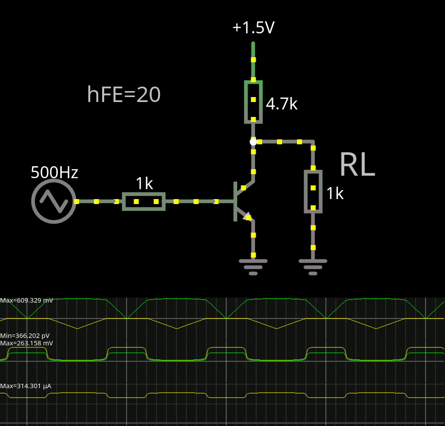
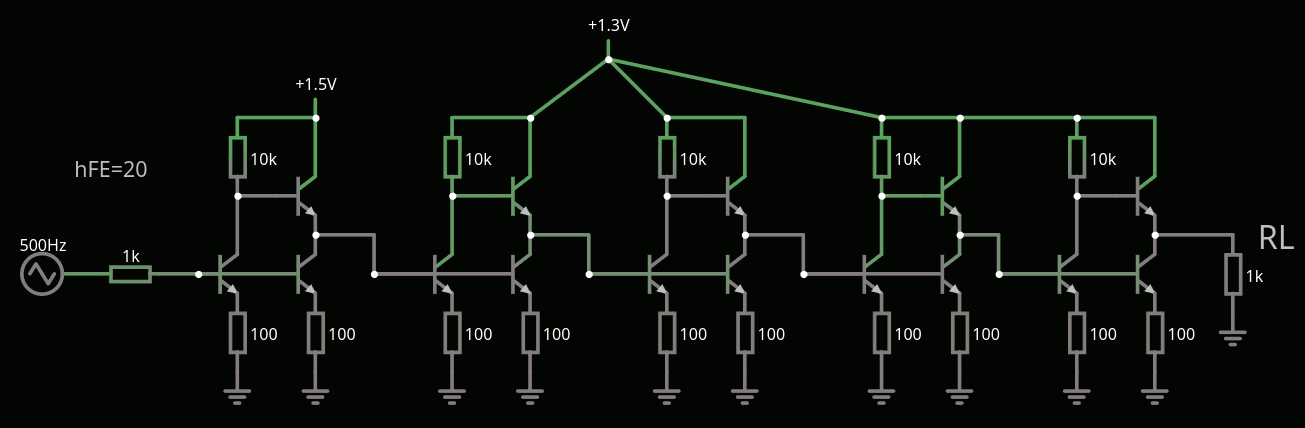
The first thing is to remove the pull-up resistor and swith to push-pull topology. For this, 2 more transistors are required : the first is a high-side common collector (like ECL), and the second is directly tied to the input, to control the base of the emitter follower.
There are 2 transistors doing the same thing in parallel (sharing the same base) because they drive different things that would not work if tied together. So we get to the 3-transistor push-pull:
It's more efficient but now there are 3 semiconductors so it was not considered in the first era of computing because of the price of a single transistor. In the late 70s, the cost per junction had started crumbling to a level that made this possible (as the ECL boom has shown).
There is no significant difference on the traces because the RL is too high, and the speed too slow to show any parasitic effect... Also due to the emitter follower, the output can only go up to Vcc-Vbe, or about 0.75V in the above example. It's higher than the 0.26V of the first example but under a low Vcc, the swing is narrow...
But 0.6V of data swing is good enough if the circuit works at low voltage because this also reduces the power draw (as seen in the DCTL experiments of the previous years). Power is turned into heat and a lot of problems so working with low voltages is good (and this is even better with Germanium transistors hahaha).
The next step that IBM took was to turn this gate into a non-saturating circuit. There, it gets to another level of analog wizardry but experience with ECL helped me unravel this a bit.
The point of avoiding saturation is to keep the transistor able to switch as fast as the input signal, and saturation stores charges in the Miller equivalent capacitor of the base. The 2N2369 was designed to reduce charge storage but this did not scale in higher frequencies and other parameters. So the transistors must be kept in a sort of equilibrium, which consumes current, but not too little or too much. The absence of resistor values in the only schematic available was annoying... I also chose low-hFE transistors because it tends to decrease with the speed (and/or the current). The germanium PNP AF240 has a hFE around 20 or 30 so it should be representative.
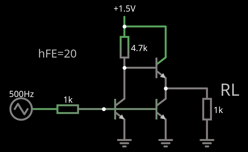
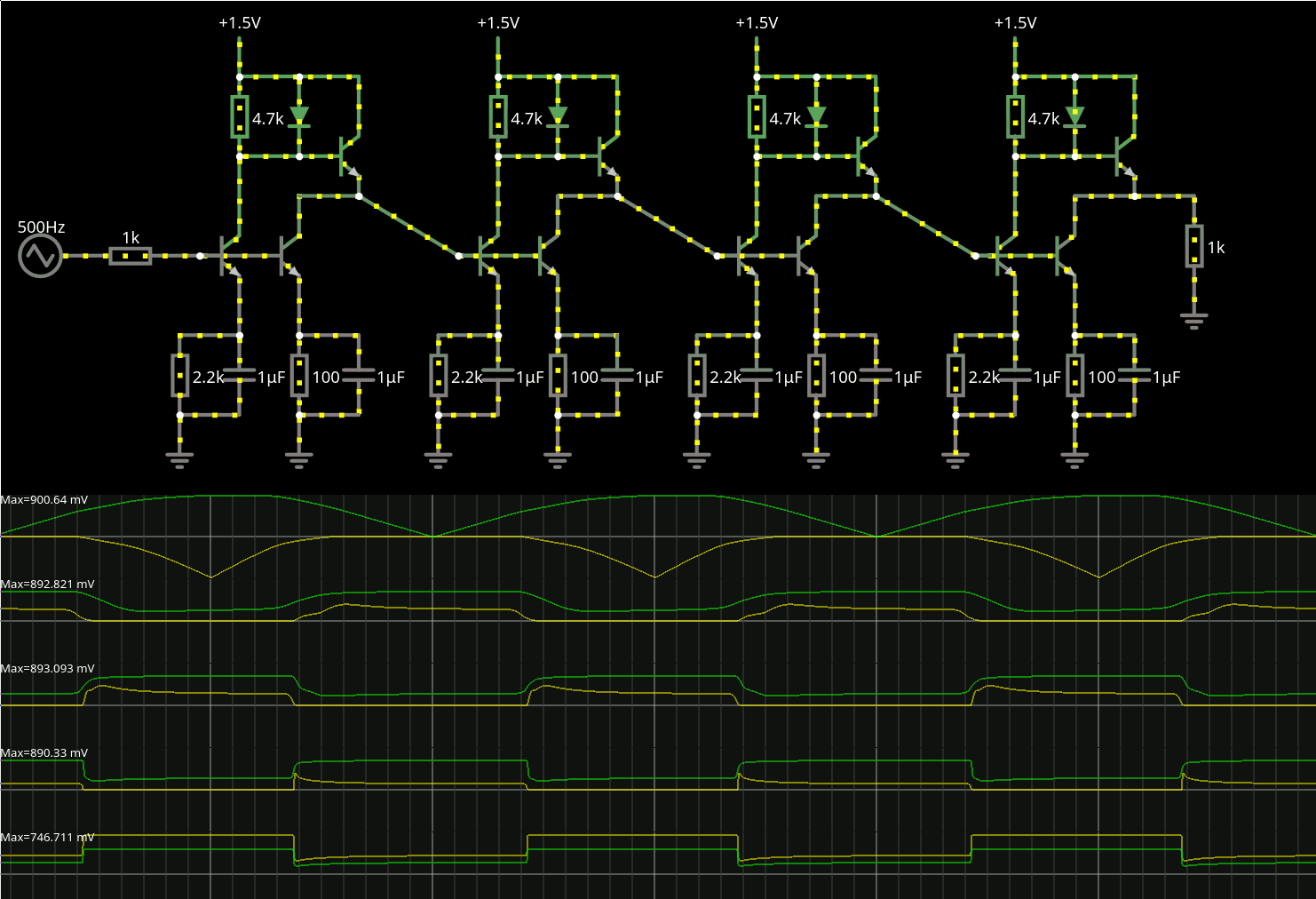
A particular detail of the original schematic is the diode in parallel with the resistor : this limits the output swing as well as the saturation (I suppose). That's the key to any change to the input-output level compatibility because the clamping must be changed when the Vcc is changed. For now I have chosen 1.5V but at 2Vcc, a second diode is required in series.
I was not able to meaningfully test the interaction of the RC cells at the legs, I suppose that the diode makes the emitter resistors conduct more current and shift the base (degeneration), keeping the input from saturating the transistors. Also I don't know why the RC are duplicated, maybe to fine-tune the values and reduce the power.
So the next schematic is the previous one with 1 more diode and 2 emitter resistors. The capacitors become meaningful at very high speed so I don't show them at such a low speed.
The following circuit chains 4 LVI inverters to ensure that impedances are matched:
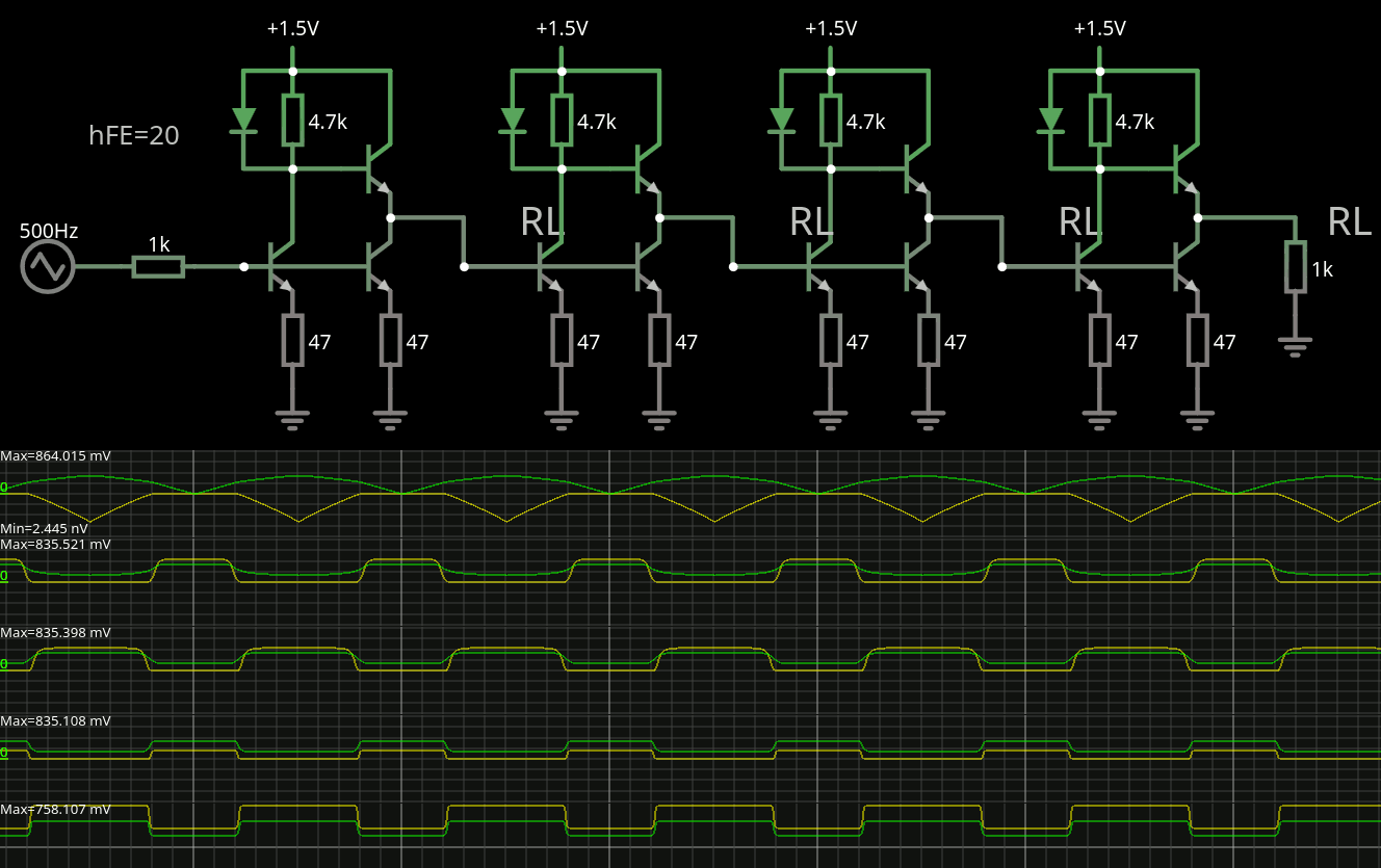
The signals swing from 346mV to 835mV. The input is a triangle (current-limited by a resistor) that gets correctly reshaped by the first inverter stage. The last stage is a pull-down load that shifts the swing down to 344mV-758mV with 758µA.
The output levels seem reasonable and quite stable. Input current is about 430µA for high level, and almost 0 for low level.
The problem is the diode that passes quite a lot of useless current and each inverter is pretty greedy, at least with the above values of 47 ohms per degeneration leg.
There are 2 ways to reduce the current : drop the diode, and the Vcc can go even lower. There is a risk of saturation though. But the power is greatly reduced.
Or increase the Vcc and increase the degeneration resistors to limit the diode's current and... This reduces available current for output. That's where the capacitors enter the stage to compensate during the transients. The gates are rated by IBM at around 1mW under 2V approx. That's 500µA max per gate.
The pull-down transistor should have a low resistance to ground to quickly drive the output low. Let's try 47 ohms. However the diode side should limit the current to 0.5mA and the diode drops 0.6V already so R=U/I=1.4/0.0005 or 2.8Ko ohms. And that's where I see that the leg resistor of the leftmost inverter can be greatly increased.
The presence of the diode increases the current but also greatly reduces the signal's swing and that's probably one key to keep the transistors in the linear region : faster speed comes from less swing and little stored charge. But now the signal integrity is harder and the imbalance of the resistors creates a new concern : the upper and lower sides should now be able to conduct at the same time. Watching the current from Vcc shows the system is safe though.
The type of diode also has an effet : low-voltage High Frequency type (low capacitance) is required, since the gate is advertised in the 200ps range... Even selecting the 1N4148 in the simulation affects the waveform compared to the "default model".
Falstad's circuitjs is not suitable for high frequency simulations so I can only check the power, logic levels, waveforms... I can cheat by adding large capacitors for example but SPICE and real circuits will give the definitive answers.
Here are the waveforms with 4 inverters with diodes: Each inverter draws either 3mA or 230µA @1.5. That's maximum 4.5mW per gate, still 5× the promised consumption but that's 10x better than the 44mW reached by log 24. Beyond 2ns with 2N2369A.
Of course the values are not "right", I focus on the resistors to get the proper working point. The capacitors will have a small value, probably in the tens of picofarads, equivalent to the Miller capacitance of the transistors.
The waveforms above show that the edges are rectified and enhanced, from the altered triangle to the clean edges of the last inverter.
Going from the inverter to the NOR gate is easy : duplicate all the switching parts. Here is the NOR2 version with the2 pairs of transistors sharing one emitter follower:
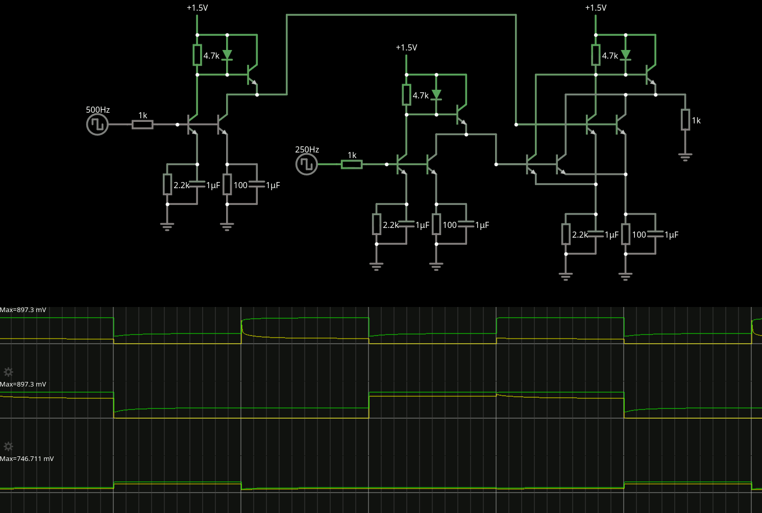
To ensure a proper input level, I reused the inverters for impedance adaptation. Here is a more succinct version : the degeneration resistors are 1K5 and 330, the lowest resistor sets the maximal static current (here about 1.3mA, or 2mW). The capacitor will affect the dynamic behaviour.
Of course NOR3 has 3 pairs of transistors. I hope that the initial schematic is now easier to understand.
Discussions
Become a Hackaday.io Member
Create an account to leave a comment. Already have an account? Log In.