 Yann Guidon / YGDES
So the last log 27. Reconstructing IBM's LVI (Low-Voltage Inversion Logic) was a lot of food for thought, and after looking back at other logs, a few ideas matured.
- I would like the gates to consume little power, ideally around the 1mWballpark. Most gates run in the 10mW range (and more, @Tim got to 44mW and that's still an order of magnitude too high for my tast, sue me).
- I would like to use the AF240 : PNP Germanium metal-canned transistors, because that's badass.
- To fulfill the 1) and benefit from 2), I set the power supply to 1.5V. Though it could be lowered later but Falstad doesn't let me use a Germanium model.
- I drop the Baker clamps. Instead I try the "non-saturating" approach of ECL and LVI and this is where things become interesting. In fact it looks quite a lot like a HF inverting amplifier stage and in the end, that's pretty close to what we do, right ?
- I drop the choice of ECL because the power supply would be too high (due to several factors). Instead LVI is a bit simpler and a bit less fussy.
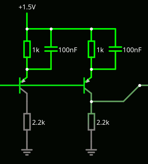
LVI gates have been already studied and it's interesting because it's easier to tune for a given power draw point. The first thing to observe is that a LVI gate combines 2 sub-parts :
- A classic inverter
- A 2-transistor amplifier with emitter-follower output.
The cool aspect is that both parts reuse more-or-less the same design for the parallel transistors (with shared base). So I can start to design the inverter first, set a given power draw, and duplicate it for the emitter follower half.
A bit of tuning later, I get this inverter:
So this almost acts like an inverting amplifier with a swing (in this very case of fanout=1) of 550mv-1100mV (centered around 850mV).
The base current is limited (to about 500µA) by the 2.2K resistor of the previous stage. The other resistor is set to 470, and together they limit the overall current. There is no direct path to ground so the power can be kept in check.
The 470 resistor is pretty critical, not just to set the working point. It also provides some degeneration, which increases the sensitivity of the base, giving the above 550mV logic swing. Furthermore the capacitor adds some more hysteresis, increases the gain temporarily, its value should not be too small (above the equivalent Miller charge, and I don't count fanouts). The overshoot on the traces above are good signs. This "boosted degeneration" is characteristic to the LVI gates and I have not seen it in other discrete deconstructions/reconstructions. Maybe this could help the DCTL gates too ?
My concern is that the Germanium transistors have a lower Vbe and possibly a smaller swing, and I can't simulate it with Falstad's Circuitjs. I'll have to try by myself on the bench, maybe by increasing the 470 to 1K. The maximum draw I want on the 1.5V supply is 2mA, and for now I measure 750µA in active state, or 1.3mW, which amonts to 0.65mW in average.
_______________________________________
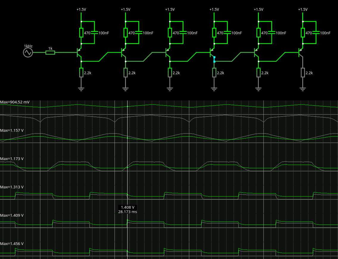
The next step is to duplicate the inverters, so the 470 is doubled to 1K to keep the base current low. The low Vcc is great because the resistors still have a rather low value, reducing the output impedance while also reducing the power losses through the resistors.
The above gate has a max. draw of 1mA, or 1.5mW (0.75 at 50% duty cycle), it's quite good so far, but the 2.2K resistors must be deduplicated. Adding the emitter follower brings the new topology:
the yellow trace at the bottom is the supply current : it peaks at 1.8mA but settles to 650µA, that's right 1mW !
The emitter follower has a swing that exceeds 0.7V, indicating saturation, so a diode could smooth this a bit and prevent transconduction of the push-pull stage. Adding a 1N4148 increases the plateau to 750µA and the peak to >4mA so the speed benefit better be significant. But I don't see a significant difference. Another more interesting effect is obtained by setting all the resistors to 1K, as this helps discharge the base faster from the emitter follower.
___________________________
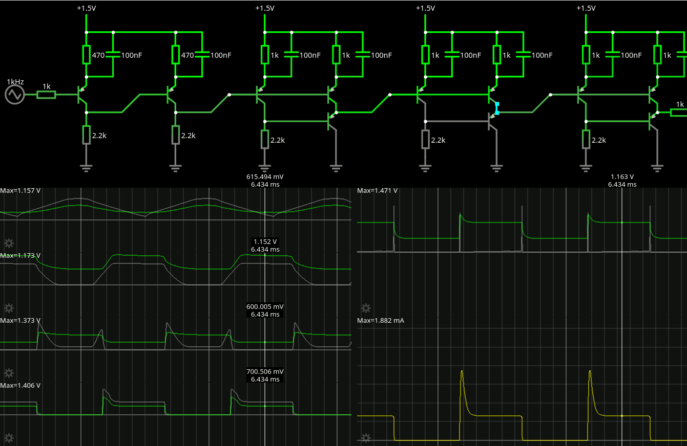
So here is the playground:
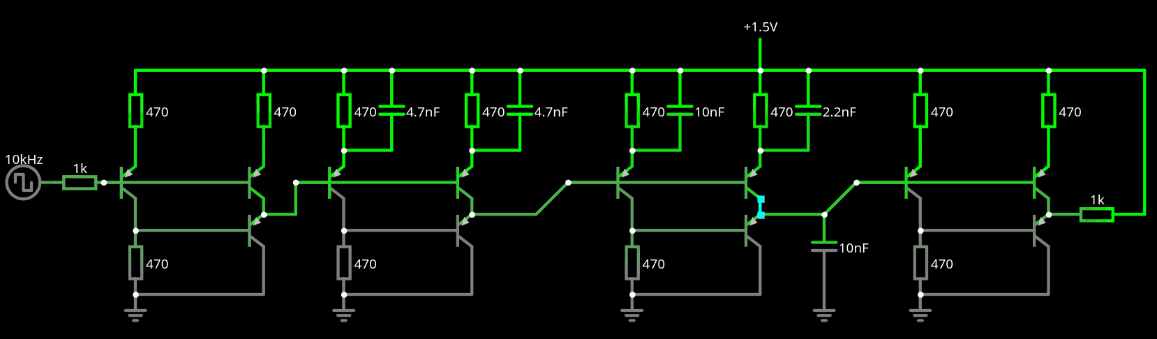
I can play with Vcc, measure the inverter's power, compare the reactions with various capacitances... The push-pull's capacitor helps increase the swing but the other one can be a bit larger, though being equal is good too. The push-pull works nicely when dealing with capacitive loads (such as long wires). The boost capacitors must be at least equal to the load.
The signal swing is about 400 or 500mV, which is not much but cascading the gates seems to be OK (I observe the 3rd in the chain to make sure the signal characteristics are pertinent, input and output).
The above circuit seems suitable for use with high speed bipolar transistors (like BFS480 or BFP420) but the speed must be measured, without and with capacitors of various values.
The AF240 would run at 1.3V or 1.25Vcc so I can regulate with a LM317 directly. I'll have to compare the latest version with the original "balanced" inverters, to see which is fastest. Saving a couple of transistors would be nice right ? but LVI shines when the output load increases so higher fanouts become possible.
Discussions
Become a Hackaday.io Member
Create an account to leave a comment. Already have an account? Log In.
Interesting, I completely missed these logs when you wrote them.
This gate type looks fairly analog, basically a common emitter amplifier with push pull output and reach through cap. I guess the only "digital" thing is the diode that prevents the pull transistor to turn off.
Are you sure? yes | no
I have only implemented the inverters, the NORs are more boolean :-)
that would be the next step in the redesign of the gates.
Who's interested to explore that ?
Are you sure? yes | no