Log book of FPGA adventures at home
To make the experience fit your profile, pick a username and tell us what interests you.
We found and based on your interests.
Lately, I've been working on getting a JTAG for FPGA infrastructure up and running.
The goal of this is two-fold:
The first installment simply talks about a small JTAG controller GPIO block that can be used to replace Altera's In-System Source and Probes debug block.
The first article in the series can be found here.
In an earlier log, I already wrote about needing a microscope to solder probe wires onto the pins of a TQFP 144 package.
The microscope in question is a Bausch and Lomb StereoZoom 4. There’s a really good article about this microscope here, but the gist of it is this:
The article linked earlier goes in quite a bit of detail on how to calibrate and align the eyepieces etc. This was not necessary with the one that I bought. All I had to do was make some minor adjustments for my left eye.
An original manual can be found here.
There are two kind of stands:
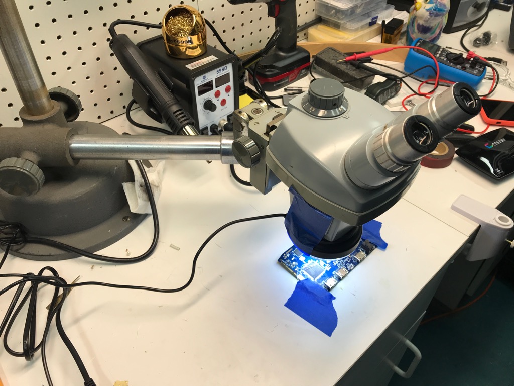
The most common configuration comes with 10x eye pieces. With the main body magnification going from 0.7x to 3.0x, that gives a total magnification from 7x to 30x.
My scope came with 15x ehye pieces instead. I don’t think it makes a huge difference. When soldering, I also keep the scope set at the lowest magification: 0.7x.
eBay or Craigslist!
As I write this, there are tons of them available on eBay.
They are offered with a boom stand, regular stand, or no stand at all: just the body, in which case you need to buy one separately (or improvise and make your own?)
Prices are absolutely all over the place.
Having followed a bunch of auctions on eBay, it’s clear now that I got mine for an absolute steal: $95. Similar configurations sometimes go for $200 and more: $550, even $800. (For these kind of prices, you should be able to find much better soldering microscopes, such as old models from Vision Engineering.)
Boom stands go for $50 to hundreds of dollars on eBay.
You don’t strictly need an illuminator: a lamp on the side will work fine. In fact, when using the phone adaptor, I found that I got best results with the illuminator switched off: the LED light would refect off the metal of the pins and the phone couldn’t really deal with that. However, when not using the phone, it is simply so much easier to get exactly the right amount of light and change the intensity as needed.
At the bottom of the main body is a recessed ring in which you can screw an illuminator adaptor (or additonal lenses as well.) This ring has a diameter of 1.5” or 38mm. Most illuminator rings that I could find on Amazon where from AmScope which expects a recessed right of 48mm.
However, you can find an AmScope to StereoZoom ring adaptors that will convert from 38mm to 48mm … for $35 and up.
I ended up buying a $25 64 LED AmScope ring illuminator and I use painter’s tape to attach it to the microscope. It’s ugly, but it works.
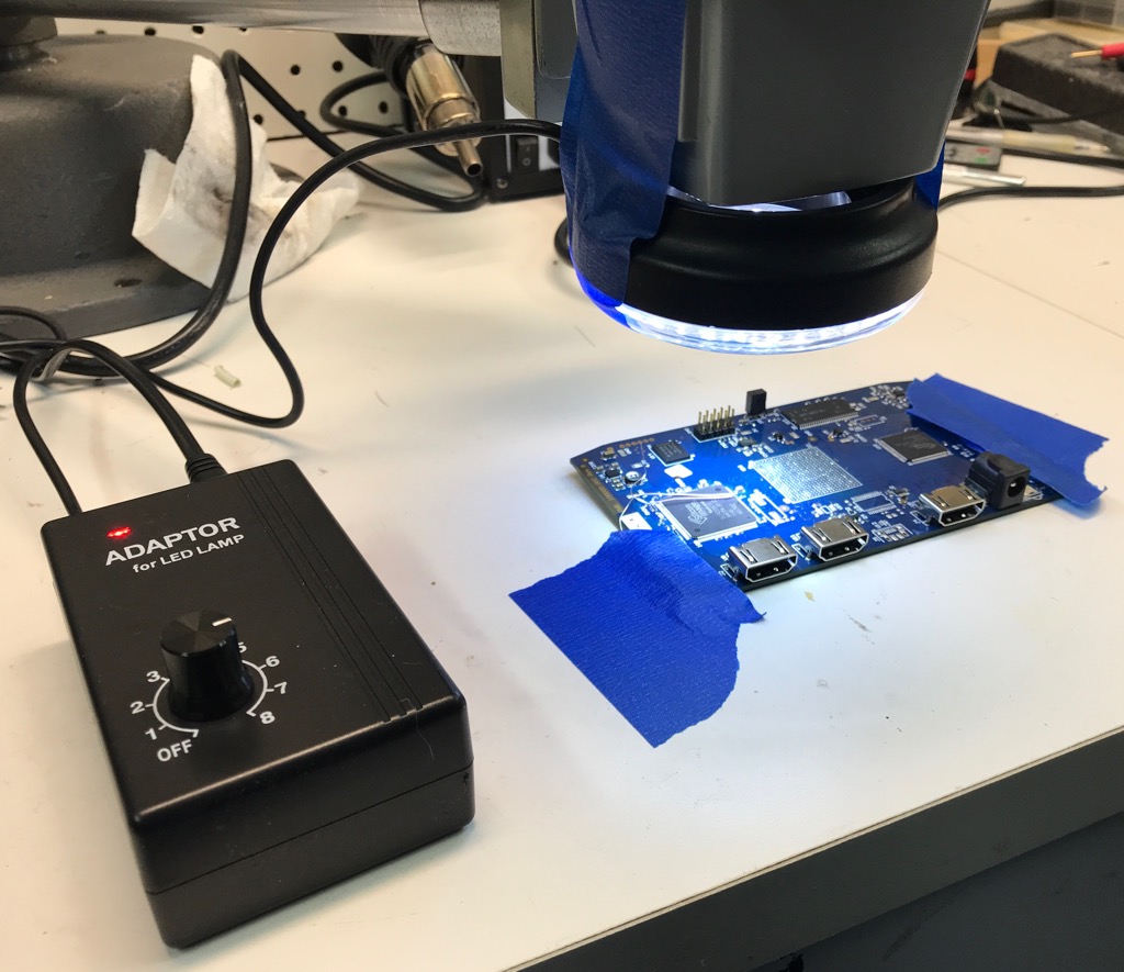
I wanted a mobile phone adapter for two reasons:
There are two main options: some holders simply make it possible to hold the phone in front of the existing eye piece. Other models have an eye piece themselves.
I bought both to compare them. The ones with eye piece cost about double ($22 vs...
Read more »I have a few projects going on that require reverse engineering the command stream between different chips. For example, in my eeColor Color3 project, there is no programming documentation of the I2C registers of the Silicon Image SiI9233.
So one way or the other, I need to probe the I2C bus of this chip.
The good news is that the chip has a TQFP144 package which means that the pins are out in the open. The not so great news is that TQFP pins are spaced 0.5mm away from each other.
My initial plan was to buy some very small probes that can connect to those pins. The second plan was to solder wires on the pins.
In the end, the second plan worked out great and was completed long before I could try out the first plan, but since the wheels of the first plan had already been put in motion (I had ordered the probes), I might as well share my experience with those little probes.
If you want to go the high end route, you go to Pomona Electronics or ProbeMaster.com where you’ll find a number of options.
A good example are these SMD grippers. I’ve used them at work. They are spec’ed to grip pins that are 0.5mm away from each other. They also cost $39 per gripper. Ouch.
There are two cheaper options, such as another pair of SMD grippers (at $9 each) and a set of 10 (at $12 each).
Having used similar of these grippers as well, they are clearly of lower quality than the first ones. If you absolutely need these kind of probes (and your employer is willing to pay for them), just spend the money.
But for a hobbyist, they are too expensive.
Much cheaper, $5 each, are these Pomona grabbers on Adafruit. They seem to be an excellent choice for SOIC packages, but are probably too big for my 0.5mm spaced TQFP144 pins.
So let’s get over to AliExpress and see what’s available.
You’d expect there to be plenty of alternatives, and you’d be wrong. I may have been using the wrong keywords to find the right product, but the smallest grippers are for SOIC-type packages (which have a pitch of around 1.2mm.)
Until I stumbled on the Micro Chip R/W Clip. Surprisingly, they are marketed as a tool that allows you to reprogram a car remote control key IC. Including shipping, they go for about $15. $1.5 per probe, not bad.
3 weeks after ordering, the following box arrived at my door:
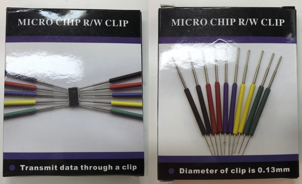
The package has the follow contents:
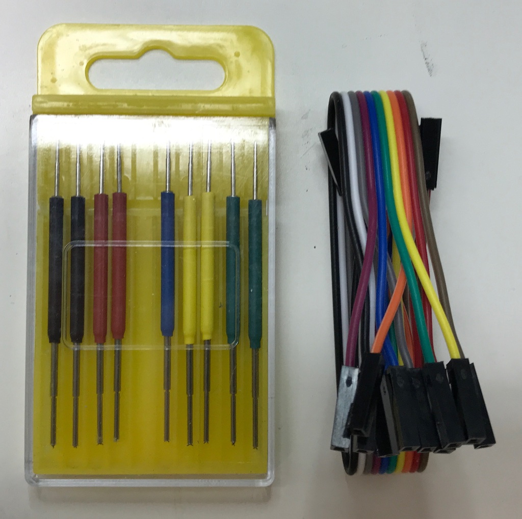
The grip of the probe is surrounded by a long and a short side. The long side is the one where the clamps will come out. The short side can be pressed in to push the clamp out. The metal of the probe has a transparent plastic layer around it:
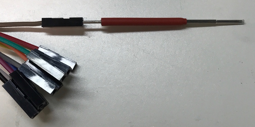
Unlike the high end grabbers, there is no easy way to push on the short end of the probe: it’s too sharp to press with your bare finger. Instead, you need to plug in the black connector and then press on the connector. However, even if you do that, the black connector will come loose from the wire that’s inside it. So you actually have to push on the connector and the colored wire at the same time.
It’s not super practical, but it works, as long as you have your two hands available: one to hold the probe, the other to push.
So how do they work in practice?
Here’s a small example where I connect a probe to various pins of an SDRAM:
The 54 pin TSOP has the pins spaced 0.8mm from each other. It’s clear that probing a single pin is pretty easy.
Probing 2 adjecent pins is a bit harder but it’s definitely possible as well:
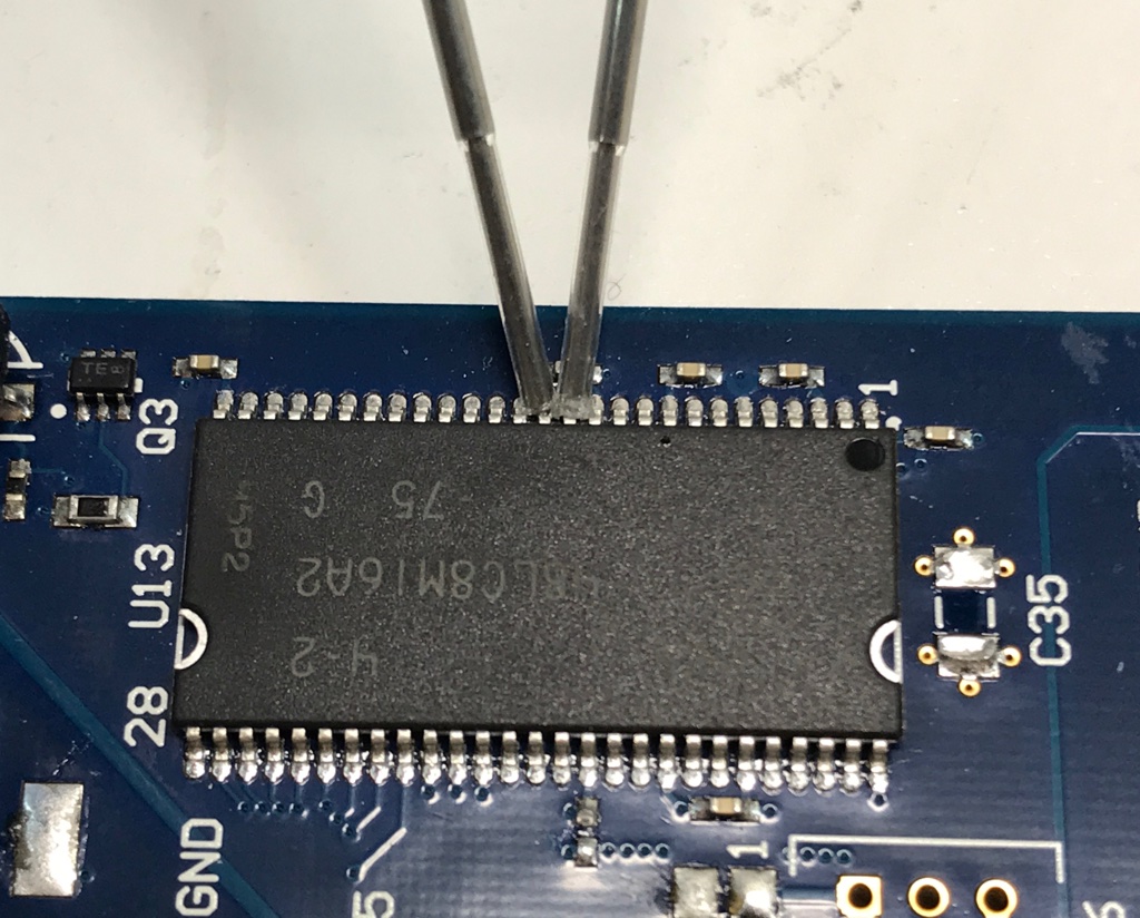
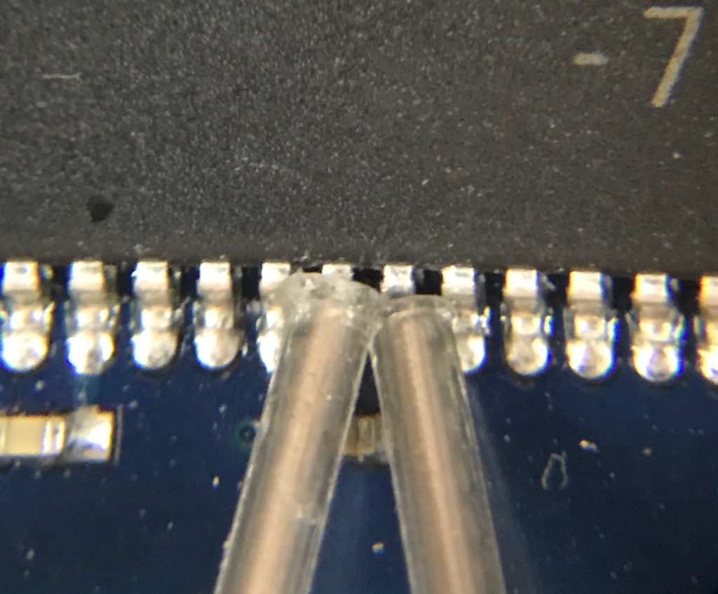
But that’s about the limit: the probes themselves as just too wide reach 3 closely spaced pins.
Finally the case that started it all: probing an I2C bus on a TQFP 144 package.
It takes a little bit of effort, but probing a single pin is very doable:
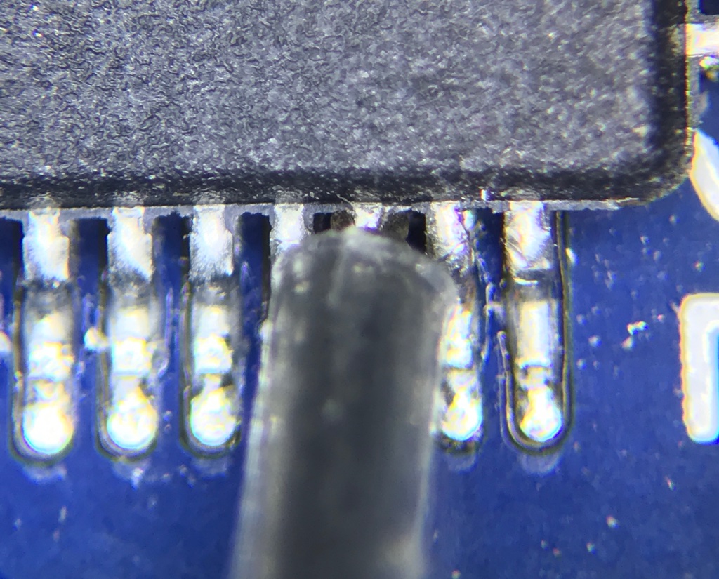
But that’s where it ends. If we zoom in a little bit more, we see the grabbers of...
Read more »(Also published here.)
I was supposed to work on getting the SiI9233 up and running, but UPS delivered a nice package today:
I had an urgent need to measure something meaningful.
Since I don't have a microscope (yet) to solder some really tiny wires on the TQFP144 of the SiI9233 (I want to record all I2C transactions to see how the thing gets configured), I decided to have a closer look at the difference between a high quality $50 Terasic USB Blaster and the cheap $3 Chinese clone that's available on AliExpress, eBay etc.
The Terasic version is supposed to be an Altera sanctioned design that has a chip USB to parallel converter chip from the FTDI family, and a small CPLD that converts the parallel data into JTAG (and some other formats).
The Chinese clone contains an STM32F101 micro controller.
As I wrote earlier, the biggest issue with the cheap clone is that it doesn't work on my eeColor Color3 board.
So let's look at the signals as measured on the JTAG connector of the Color3 board.
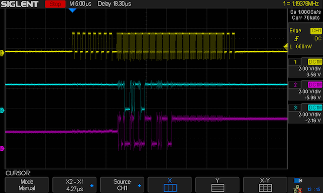 This is the first transaction that travels over the JTAG cable when you issue the "nios2-terminal" command.
The most important signal here is TCK, in yellow.
There are 3 major sections: during the prefix there are 8 slow clock cycles. In the middle there are 16 groups with fast clock cycles (each group is itself 8 clock cycles). And at the end you have a suffix with 2 slow clock cycles.
For this investigation, it doesn't matter what gets transported when, but it's almost certain that the slow clock cycles are used to move the JTAG TAP from iDLE state to the scan DR or scan IR state, and that the fast clock groups are used to rapidly scan data in and out of a scan data register.
When you zoom in on the slow clock cycles, you can measure a TCK frequency of 780kHz: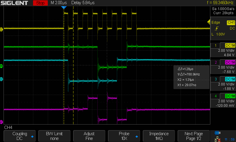
Meanwhile, during a fast clock group, the clock toggles at 6MHz. This is expected: according to the Altera documentation, 6MHz is exactly what one can expect from a USB Blaster.
In addition, there are roughly 3 idle cycles between a fast clock group.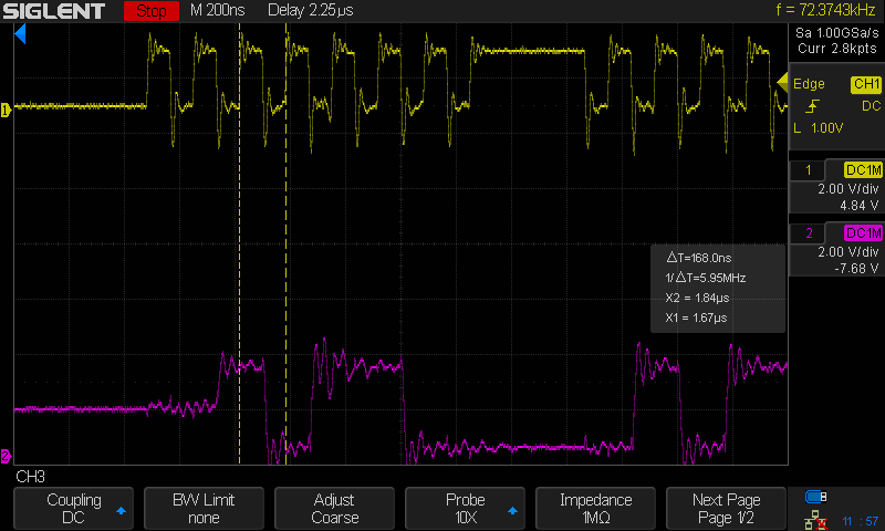
And here's the equivalent of the cheap clone. For the overview, look at the upper set. The set of signals below that is a slightly zoomed in version of the one above.
We see a similar pattern, but interestingly enough, it's not the same.
We have a prefix with 8 slow clocks, but in between the second and the third slow clock, there's a signal fast clock group.
In the middle we have the expected 16 fast clock groups.
The suffix is really different, with 6 clock clocks but also a fast clock group in between.
While the Terasic was rock solid in its communication with the Color3 board. The cheap clone was never able to get reliable contact.
Zooming in on the slow clocks, we see a clock frequency of 192kHz.
A fast clock group sets the clock at 12MHz instead of 6MHz.
A really interesting difference is in the spacing between fast clock groups: for the Terasic, it was around 3 fast clocks (roughly 3x16us=48us). For the cheap clone, the spacing is huge: around 40 clock cycles (40x8us=320us).
If we ignore for a second that the cheap clone doesn't work on this particular board, the biggest consequence of the chapeau clone is that bulk transfers are much slower: (8+3)x16=176us per byte vs (8+40)x8=384us per byte.
It looks like the cheap clone is able to squeeze out bits really fast, but there's quite a bit of software overhead in processing the next byte in the USB packet.
The Terasic doesn't have that problem: there is no software. All processing is done with a simply state machine.
What remains is the question about why the cheap clone doesn't work. It's not that it's broken: the clone works fine on my EP2C5T144 mini development board. My money is on the clock speed: even with the Terasic, the signal isn't super clean, and the one of the cheap clone looks...
Read more »(Also published here.)
Dirt cheap USB blaster clones considered harmful... or at least non-functional.
My very first hobby FPGA boards was the popular EP2C5T144 Mini System Learning board with the smallest Altera Cyclone II FPGA. You can find them for $12 on AliExpress.
To program the board, you also need a USB Blaster: Altera's version of a JTAG cable. These, too, can be found on AliExpress for less than $3. It's really a steal. (Identical copies sell for $10 on Amazon.)
I've been able to make this cable work with the EP2C5 board so I thought it was all good.
However, I'm now in the process of reverse engineering the eeColor Color3 board (which conveniently has the JTAG connector still populated), and I spend more than an hour trying to get it work. Quartus was able to detect the USB Blaster, but most of the time it didn't even detect the JTAG chain. And if it did, it'd detect the wrong JTAG chip ID. And I never managed to get a bitstream programmed.
Now what?
Well, you try out another JTAG clone: : the Terasic USB Blaster. It sells for $50 on the Terasic website and $70 on Amazon, which is still $230 less than the official real thing from Altera.
I plugged it in and ... voila! ... everything worked like a charm.
I suspect that the dirt cheap ones have really crappy level shifters (if they have them at all.)
(Also published here.)
I'm taking a short break from the BlackIce-II to spend some quality time in my garage with the eeColor color3. Originally a real consumer product built with a Cyclone 4 FPGA, a DRAM, an HDMI receiver and an HDMI transmitter, it got its 15 minutes of fame when it was featured on Hackaday as a potentially really cheap FPGA development board.
A few people mapped out the IOs of the FPGA and built a bitcoin miner with it, but I'm not aware of any projects that are using all the features of the board.
Today, most color3 boxes sell for $20 and more (+shipping) on eBay, but I was able to grab one for just $10+shipping.
It'd be a shame if the scattered reverse engineering information of the color3 that can be found on the web would disappear due to standard web-rot, so I've started a Hackaday project and a github page to gather all the information I can find today, and, hopefully, also document my own progress in getting all the chips to work.
My larger goal is to create a new firmware called "icehub" , which will enable a bunch of new development features. Instead of using the standard ST libraries, I want to use libopencm3 instead: it's an open source library that works with most Cortex based SOCs and microcontrollers.
Today, I wanted to create my first libopencm3 program, a blinking LED obviously, run it on the STM32 of the BlackIce-II board, and step through it with the debugger.
After yesterday's success of getting the Blue Pill to connect to the Blackice, this certainly wasn't going to be overly complicated! Right?!
libopencm3 has support for "stm32l4", but only a few specific types. Our L433 was of course not part of the list.
Adding support turned out to be pretty easy: you just need to tell how much ROM and RAM it has and add that information to ./ld/devices.data.
There are a lot of examples as part of the library, and there's even an l4 directory for that, but a shared Makefile is missing. So that had to be fixed as well.
After this, I could compile the "libopencm3-examples/examples/stm32/l4/stm32l476g-disco/basics" example.
(I need to commit those changes and create a pull request for that.)
Since I ultimately want to do a lot of USB-related stuff, I started with a usb_cdcacm example from the F1 examples directory. This forced me to start digging into the whole clock architecture of the STM32, because the F1 is really different there. Not the most efficient way to get to blinking LED.
Anyway, eventually I ended up with something that compiles.
On the BlackIce-II board, the DBG1 LED is the only one that can be controlled directly by the STM32, so that's the one!
This is where I ran into a crucial limitation of the Black Magic Probe: it doesn't support flash operations!
So I changed the address map to create a binary that is mapped to address 0x2000_0000, the RAM of the STM32. And it gets loaded fine there. However I could not figure out to get GDB to execute from an address in that range.
I needed a different solution: my original STLink v2 dongle!
After yesterday, I'm a wiser man now, so I added an extra GND wire between the STLink and the BlackIce board, I fired up openocd, and *HURRAY!* it connected just fine!
What's more: when you telnet into openocd, you can issue flash read and write operations!
And that's what I did:
What's more: the LED was blinking correctly right away!
Ultimately, I would love to debug my programs from RAM instead of flash, but for now, I'm moving back to using the STLink instead of the Black Magic Probe.
In yesterday's log, I wrote about not being able to connect the STLink v2 to the STM32 of the BlackIce-II board.
Right now, that still doesn't work, but I found a work-around: I installed the wonderful BlackMagic Probe firmware on the Blue Pill STM32F103 board, which converts the Blue Pill into a debugging dongle that's actually more powerful than the STLink v2!
An STLink v2 is essentially a protocol converter from USB to SWD. You still need OpenOCD as an intermediary to link GDB to your STM32.
Not so with the BlackMagic Probe: it has acts like a serial port on the USB side, has a GDB server built-in which drives a SWD or JTAG interface. OpenOCD is not needed anymore: you connect your GDB straight to the dongle.
How did I get there?
This turned out to be a combination of this article: "Converting an STM32F103 board to a Black Magic Probe"and this article: "Programming an STM32F103XXX with a generic "ST Link V2" programmer from Linux" (which I already reference earlier.)
The first article assumes that you don't have an STLink v2 dongle and compiles then installs the BlackMagic firmware using a USB to Serial dongle instead. The second one tells you how to install anything with the STLink dongle.
I wanted to use the STLink dongle to install the BlackMagic firmware.
All in all, the procedure was pretty straightforward.
In the process of all this, I learned a little bit about this all works:
I wired the following signals:
Once you have BlackMagic Probe running on the Blue Pill, you can connect to it directly with gdb:
I want to use my BlackIce-II board as a development and debug board for designs that can later on be moved to an FPGA-only design, where the STM32 provides a bunch of support features.
For example, the STM32 could be used to load a new bitstream, be a JTAG master to the FPGA (when you put a TAP in the FPGA), drive QSPI if you need the transfer speed, etc.
To make that work, it's really necessary to be able to use GDB during the STM32 development.
For that, you need an STLink v2 dongle that supports the Serial Wire Debug protocol. Turns out: these things are dirt cheap. You can get them on AliExpress for as low as $1.80 if you can stomach a 30 day shipping delay.
While looking for those, I also noticed an abundance of ridiculously cheap STM32F103 development boards. They go for $2.50 on AliExpress as well. (These boards are also advertised on eBay for the same price, but they *also* take more than a month to arrive.)
I didn't want to wait that long, so I bought the STLink + STM32F108 board for $12 or so on Amazon. $8 extra meant I had the thing at my doorstep 2 days later.
Why the STM32F108? Because I already have a pile of micro controller boards. Why not have one more?
But also: there are plenty of tutorials on the web on how to get that board working with the STLink dongle and OpenOCD. So for just a few dollars more, I can replicate exactly the same configuration before I move on to great things.
I'm glad that I did.
I followed these instructions and, after swapping two wires, I had the thing going and was able to dump the contents of the STM32 flash contents. I'm currently not all that interested in getting C code to work on that one, but it should be pretty trivial, I think.
My drawer has a bunch of ATmega1280 boards from a previous life, an Adafruit Feather board with an ATmega and BLE, an LPC<something> board that I bought to see if it was still possible to an ARM7TDMI up and running (no issue with today's open source tools BTW), an Nvidia Jetson TK1 board, and some others that I'm forgetting.
But none of them are as cheap as this little thing. And it way faster than ATmega based products. If you want get into this kind of tinkering, and you want to do it cheap, these STM32F103C8T6 are absolutely the way to go.
Anyway...
Next step: getting it to work with STM32L433 that sits on the BlackIce-II board.
While the STM32F103 works find with OpenOCD 0.9.0 that comes with my Ubuntu 16.04 installation, this is not the case for the STM32L433. You need the stm32l4x.cfg configuration file for that, which is part of 0.10.0.
I started by connecting 4 pins between the dongle and the BlackIce board: GND, SWCLK, SWDIO, and 5V, and while that *did* result in some LEDs lighting up... a little bit, the FPGA didn't really come up. So I'm now NOT connecting the 5V and using USB instead to power the board. The STLink 5V is clearly not powerful enough to drive the BlackIce board.
I'm currently still at this dead-end:
adapter speed: 500 kHz
adapter_nsrst_delay: 100
none separate
Info : Unable to match requested speed 500 kHz, using 480 kHz
Info : Unable to match requested speed 500 kHz, using 480 kHz
Info : clock speed 480 kHz
Info : STLINK v2 JTAG v17 API v2 SWIM v4 VID 0x0483 PID 0x3748
Info : using stlink api v2
Info : Target voltage: 3.234369
Error: init mode failed (unable to connect to the target)
in procedure 'init'
in procedure 'ocd_bouncer'
Connecting RST of the STLink to RESET_ of the BlackIce connector didn't work either.
So I'm stuck with that for now.
What I really want to do first is to have a multi-function interface into the FPGA with multiple virtual channels: STDIO, debugger for a RISC-V CPU, waveforms etc. If I can't get this to work, I might restore to just JTAG for a while and not use the on-board STM32L....
Read more »After laying on my nightstand for 3 weeks (during which my BlackIce-II board got all my attention), it's time to get a minimal design going.
The Upduino documentation on GitHub is a Word file that describes how to create a LED blink design with the Lattice iCECube2 software and how to program it with the Lattice Diamond programmer. I don't have those, but I decided to try if it works with Project IceStorm.
Of course, it does.
After the usual amount of struggling with command line options (forgetting to use `sudo` didn't help either), it was able to get a blinking LED going. The results can be found here: https://github.com/tomverbeure/upduino/tree/master/blink
Check out the Makefile for the right combination of command line parameters for the different tools.
Various notes:
Create an account to leave a comment. Already have an account? Log In.
Become a member to follow this project and never miss any updates
 Jared
Jared
 ajlitt
 charliex