 Rob Ward
The Sym-1 had a comprehensive expansion strategy with both I/O (3 6522 PIAs and a 6532 RIOT) and memory. The board was shipped with 1kB RAM and this could be expanded "on-board" to 8 2114 Static RAM chips to 4kB onboard. (It also allowed write protect of this extra RAM in 1kB blocks). There was also provided four 24pin ROM sockets. As shipped it had its monitor (Supermon 1.0) in a 4kB block from $8000 to $8FFF. The other three sockets were pre-wired to accept 2kB ROMs, or EPROMs.
To be able to do this configuration after shipping meant providing some ROM selection to be done in the factory but to also allow later configuration in the field. A system of address decoders (74LS145) were used that were open collector outputs and options to "OR" these together to be able to map ROMs from 2kB, 4kB and 8kB into the upper memory spaces. RAE and BASIC were both available as two 4kB ROMs or as single 8kB ROMs.
Here is an example memory map of the upper 32kB
| $8000-8FFF | SuperMon | 4kB |
| $9000-9FFF | Supermon Expansion or Extensions | 4kB |
| $A000-AFFF | Memory Mapped I/O and 128B of System RAM (Not usable as ROM) | 4kB |
| $B000-BFFF $E000-EFFF | Resident Assembler and Editor (RAE) (This has separated 4kB entries *, and note correction below ) | 4kB 4kB |
| $C000-DFFF | Microsoft BASIC | 8kB |
| $F000-FFFF | Extension area (must include ROM startup Vector) | 4kB |
In the early 1980's the 2716 EPROM (2kB) was a popular and easy to use chip and was often used to expand the Sym-1 ROM memory. These days the 2764 EPROM (8kB) is about the same numerical price or cheaper in quantity, and of course much cheaper given inflation. However a 2764 has 28 pins and not 100% compatible with the 24pin onboard sockets, but a good proposition having 8kB capacity means RAE or BASIC or Supermon+extensions could fit into a single chip (and we could fill the upper 28kB with ROM if desired). The old 2364 masked ROMs had only 24 pins, but as soon as the EPROM version is chosen it has extra pins for program enable and provision of the programming voltage (eg 12.5V etc)To get around this a riser board was made that has a 24 pin plug below and a 28 pin DIL socket on top, with the leads routed to reproduce the pin-outs functionality of a 2364 masked ROM.
Because the pin-outs of a modern 2764 are about 85% identical to a 24pin 2364 only small changes needed to be made to re-route the various signals. This is outlined in another page here XXXXX. The trick after "burning" the EPROM is getting the memory map links set up so that the EPROM appears in the right memory locations. The information in the manual is very helpful and accurate, but organised that well to instantly make clear what needs to be done. Below is the array of connections (and PCB breaks) used to implement the system above.
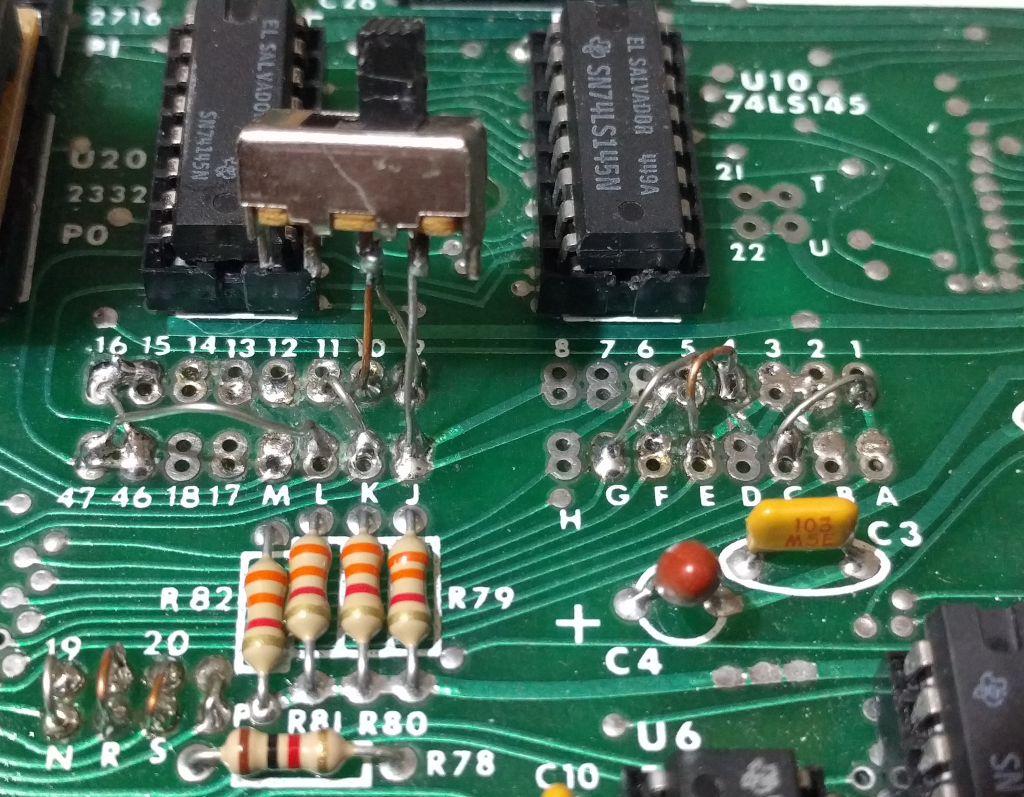
The jumpers and PCB Breaks list:
| C to 1 | Allows RAE EPROM access to A11 | ROM U22 |
| E to 4 and G to 4 | Allows Supermon +Extensions EPROM and RAE Access to A12 | ROM U20 |
| J to 10 and J to 9 (9&10 are switched to J) | Adds CS for $9000 and $9800 Extensions ROM | ROM U20 |
| K to 11 | CS for Extra ROM (not used here, eg BASIC at $C000) | ROM U21 |
| L to 46, L to 47, L to 15 and L to 16 | CS for RAE EPROM, $B000-BFFF and $E000-EFFF | ROM U22 |
| Cut PCB at C // 2 | disconnect S21 pin 18 from GND | ROM U22 |
| Cut PCB at E // 3 | disconnect S02 pin 21 from GND | ROM U20 |
| Cut PCB at G // 5 or 6 | disonnects S22 pin 21 from 5V | ROM U22 |
This is essentially enabling the high address lines A11 and A12 for the bigger 8kB EPROMS and to also free the same lines from being tied to GND or 5V (for the original 2716 chip enable OE or CS pins).
* NB: RAE Addressing QUIRK There is a quirk in the Sym-1 ROM slots. Where A12 goes to the U20 Supermon chip correctly, there is a mistake for the U22 chip position that I chose for the RAE chip. It has the A12 line inverted. What this meant was I had to split the ROM image for RAE in half and reverse their position in the 8kB ROM. So $B000-BFFF was in the second half of the EPROM and $E000-EFFF was in the first half of the EPROM. In the RAE Notes it talks of using a spare inverter on the Sym-1 board to do this inversion of A12. It would appear they did not know this themselves when they created their own ROMs. However we can simply correct for it by reversing the order of the 4 blocks and it works fine. G B000 works to run RAE and it is ok after that. I will try to add a RAE version for 2764 EPROM in the files section.
For the project overview and support files Project Page Sym-1 A 6502 Phoenix!
REF: Pages Fig 4-11 (p4-27), Table 4-3 (P4-28) Fig 4-8 (P4-15) (Sym-1 Reference Manual July 1980)
Discussions
Become a Hackaday.io Member
Create an account to leave a comment. Already have an account? Log In.