Hi, friends welcome to the new post. This post will look at the Four Layer PCB Layout: Design Process and Cost of Manufacturing. Due to its different advantages and benefits, four-layer PCB boards are now the standard for electronic circuit design. This tutorial will cover the four-layer PCB layout design process and manufacturing expenses details. Engineers and PCB designers can make PCBs that are effective and affordable while yet meeting the demands of contemporary electronic devices. so let's get started 4 Layer PCB
What is a 4 layer PCB
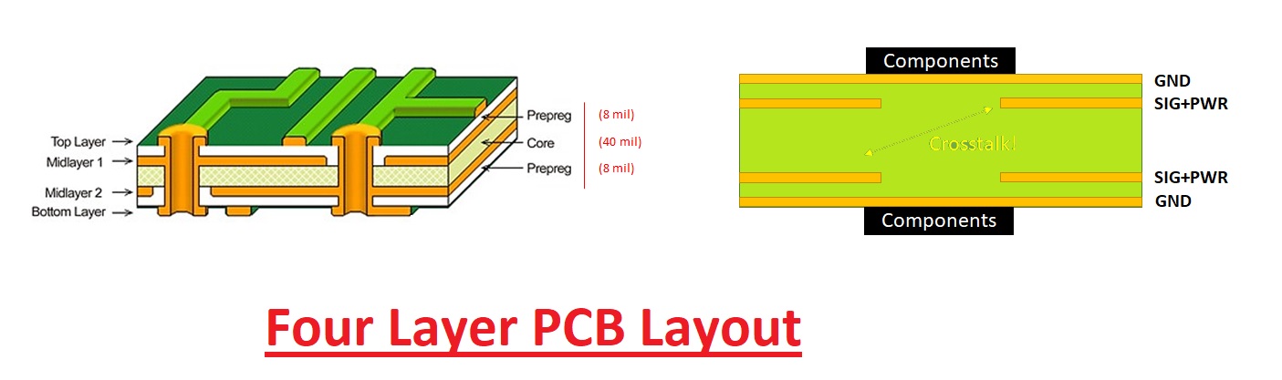
- A 4-layer PCB is a printed circuit board that comes with four layers of conductive material separated by insulating layers. It belongs to multi-layer PCB that offers increased flexibility and good performance compared to single-sided or double-sided PCBs.
[adinserter block="3"]
- In these boards, the two outer layers are typically used for component placement and routing of signal traces. These layers can accommodate many components and allow for complicated signal routing. The two inner layers, also called the power and ground planes, offer a solid ground reference and distribute power throughout the circuit.
- The power and ground planes in a 4-layer PCB help to reduce noise and provide a stable power supply to the components. They also help decreases electromagnetic interference by providing a shielding effect. The power and ground planes are interconnected using vias, which helps signals to pass between the layers.
- By having 4 layers, these board PCBs offer improved signal integrity, reduced crosstalk between traces, and better power distribution compared to other boards
2 Types of 4 Layer PCB Stackup
There are different types of stack-up configurations for 4-layer PCBs, but two most used are explained here
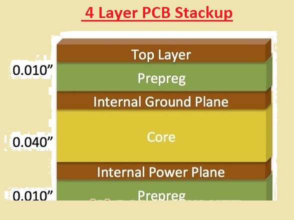
- Symmetrical Stackup:
| Description |
|---|
| Signal traces and components |
| Ground plane |
| Power plane |
| Signal traces and components |
The ground and power planes are configured in the two inner levels of this stack-up. The ground plane work as a barrier against electromagnetic interference and provides a low-impedance return channel for communications. By distributing power uniformly about the circuit, the power plane reduces voltage loss and noise. On the top and bottom layers, signal traces and component placement are done.
[adinserter block="5"]
Asymmetrical Stackup:
| Description |
|---|
| Signal traces and components |
| Ground plane |
| Power plane |
| Signal traces and components |
In this stack-up, one of the inner layers is assigned to signal traces and components, while the other internal layer work as a ground plane. The upper layer contains the signal traces and components, while the bottom layer is configured to the power plane. This stack-up allows for controlled impedance routing on the inner layer and provides a solid ground plane for noise reduction.
Benefits of Four-Layer PCB Layout:
Four-layer PCB layouts come with differnt advantages than single-layer and double-layer boards
Improved performance and signal integrity:
Good signal integrity and less noise interference are offered by the additional internal layers of a 4-layer PCB. Performance can be enhanced by designers minimizing crosstalk and maintaining signal integrity by isolating power and ground planes from the signal layers.
Enhanced power distribution:
With separate ground and power planes made possible by these PCBs, the circuit's power distribution is optimized. As a result, voltage loss is reduced, power stability is increased, and noise immunity is enhanced.
Space optimization and compactness:
Designers can get more circuit density and compactness with 4 layers, making it best for devices with a small footprint. The additional layers allow for more effective component routing and placement, which decreases the overall footprint of the board.
Noise reduction and EMI shielding:
The reduction of EMI and improvement of noise immunity are both aided by the separation of the signal layers from the power and ground planes. For high-frequency applications and delicate electronic components, this is compulsory
Four-Layer PCB Design
Creating a four-layer PCB has a systematic design process. Some steps are explained
Step 1: Schematic design:
The creation of a schematic diagram, which is a guide for the PCB layout, is the first step in the design process. The circuit's operation and component connections are configured in the diagram.
Step 2: Component placement:
Signal integrity, thermal management, and simplicity of assembly are considered while placing components on the board in this phase. A main factor in ensuring good performance and manufacturability is a proper component connection
Step 3: Routing:
Routing consists of creating conductive channels or traces to connect the components on the board. To reduce signal deterioration and interference, designers must be considered factors that are impedance management, trace length, and signal crossover.
Step 4: Plane layer allocation:
Two internal signal layers are sandwiched between power and ground planes on this PCB construction. Signal integrity and power distribution needs are considered when designers assign the proper signals and power nets to every layer.
Step 5: Signal integrity analysis:
Designers use simulation tools to do signal integrity analysis once routing is complete to check the board functionality. Potential issues like crosstalk, signal reflections, and impedance mismatches are identified by this research.
Factors Influencing the Cost of Manufacturing Four-Layer PCBs:
[adinserter block="6"]
PCB size and complexity:
Larger board sizes often needed more material, which increases production expenses. Similar to this, complicated routing and tightly packed components in complex designs necessitate additional manufacturing processes, which rises manufacturing expenses
Copper thickness and weight:
The overall cost is affected by the weight and thickness of the copper used in the board. Better current carrying capacity is given by thicker copper layers, but the cost of doing so is larger since more material is used.
Several drilled holes and vias:
The cost of manufacturing is affected by the quantity and size of vias and drilled holes. Larger expenses are a cause of the additional drilling and plating methods needed to accommodate larger holes and smaller vias.
Surface finish and solder mask options:
The cost of different solder mask choices and surface treatments differs. Finishes like electroless nickel immersion gold and gold immersion are more expensive than alternatives like hot air solder leveling. Similarly to this, high-cost solder mask coatings or colors can increase prices.
Quantity and lead time:
The production expenses can be impacted by the number of boards purchased and the necessary lead time. Shorter lead times can necessitate faster manufacture, which will increase costs, while larger volumes sometimes qualify for volume savings.
Tips for Optimizing Four-Layer PCB Layout Design:
Minimize trace lengths and widths:
Impedance mismatches and signal loss can be decreased by shortening and narrowing traces. Shorter traces further decrement the possibility of crosstalk and noise coupling.
Follow design rules and guidelines:
Manufacturability is ensured and the chances of mistakes are decreased by adhering to the design standards and guidelines supplied by the board manufacturer. Pay attention to minimum trace spacing, via sizes, and other design parameters
Use ground and power planes effectively:
Use the ground planes and power to the extent possible. It is possible to make a low-impedance power distribution network and enhance signal integrity by accurately allocating these planes.
Avoid signal crossing and interference:
Plan the path carefully to avoid signal crosses and interference. Crossed signals can add noise and decrease the board's overall performance.
Perform thorough testing and validation:
Important phases in the design process are testing and validation. To find and fix any possible issues before production, perform electrical testing, signal integrity analysis, and functional testing.
Common Challenges and Solutions in Four-Layer PCB Layout:
Crosstalk and impedance control:
Crosstalk and impedance mismatches can exist when signal traces are placed closely together. These problems can be reduced with the use of proper trace spacing, controlled impedance routing, and shielding techniques
Thermal management and heat dissipation:
Powerful components can produce a lot of heat. Overheating can be controlled and avoided with the use of adequate heat sinks, thermal vias, and component locations.
Manufacturing and assembly issues:
4 complicated layer boards can be difficult to manufacture and assemble. Effective solutions to these problems can be achieved by early engagement in the production process and collaboration with skilled PCB manufacturers
$4.5/㎡ Off on Quality 4-Layer PCBs
JLCPCB is a well-known PCB manufacturer that offers fabrication services to customers worldwide. They specialize in providing affordable and high-quality PCBs, including four-layer PCBs. By leveraging their online platform, you can easily place an order and have your PCBs manufactured and delivered to your
They are happy to announce a price decrease for 4-layer PCB small-batch orders. You can now take advantage of a special discount of $4.5 per square meter, which lowers the board fee from $75.1/m2 to $70.6/m2.
Despite the lower cost, JLCPCB never compromises on quality and upholds the highest standards of excellence throughout the board fabrication process. Examples are the full-film process for PCB manufacturing, the use of genuine A-grade substrates, four-wire low resistance via checks, advanced solder mask LDI technology, and others. Place your buy right away for fantastic outcomes on the official JLCPCB website! Every new user will receive sign-up bonuses worth up to $54.
Calculate Your Savings for 4-Layer PCBs
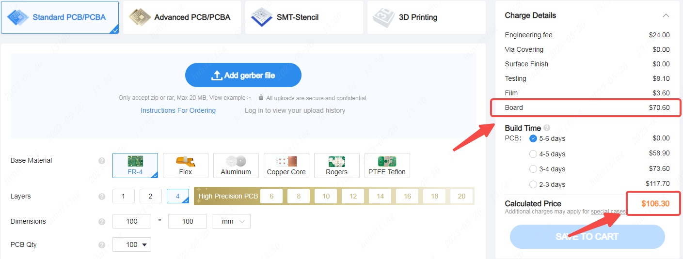
Let's use an order of 1 square meter as an illustration.
When placing an order for 100mm*100mm 100pcs 4-layer PCBs with basic settings on the JLCPCB online quotation page, you'll find that the board pricing is only $70.60 and that the 4-layer PCBs will cost a total of $106.30. Compared to the market, you might save more than $100.
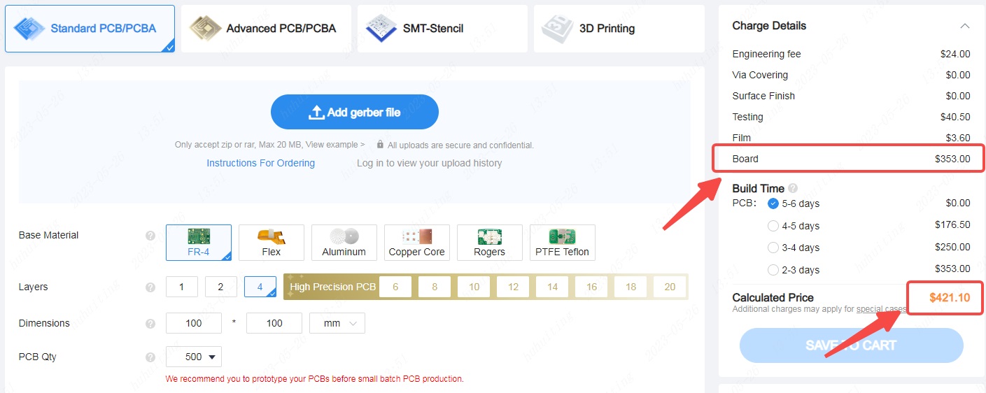
if you order five square meters.
For instance, the total cost of an order for a 100mm*100mm 500pcs 4-layer PCB with basic settings is about $421.10, with the board costing just $353. On this order, you may save more than $300 in comparison to the market. It's a rather economical decision, isn't it?
The efforts made by JLCPCB on the production side have always been aimed at helping engineers worldwide overcome cost barriers in their pursuit of innovation.
Lower Prices, Same Quality
JLCPCB is dedicated to providing affordable PCB manufacturing solutions without sacrificing the functionality, robustness, or dependability of our PCBs. JLCPCB 5 intelligence production bases, which always work to get better, support our commitment to excellence. We worked hard to improve ineffective procedures, improve the design of our PCB production lines, and put in place a fully automated intelligent management system. These current projects have produced encouraging results, especially in the small-batch manufacturing of 4-layer PCBs. That is the justification for the price drop.
JLCPCB works to impart its years of PCB manufacturing experience to engineers and producers so they may more effectively use our production advantages to their benefit.
Key Promises of JLCPCB Manufacture's Quality Focus
- Negative film is never used for the full-film manufacturing of any circuit boards.
- JLCPCB ensures higher reliability by checking vias with four-wire low resistance.
- In order to achieve equal-sized solder mask apertures and enhanced solder mask bridges, JLCPCB's multi-layer boards, including 4-layer PCBs, use LDI for circuit solder mask alignment.
JLCPCB Offers in 2023
- Flexible PCBs: $25 for 5 pcs, supports standard PCBA.
- $2 special offer for 1-8 layer PCBs (5 pcs).
- Free assembly for 1-6 layer PCBs with the monthly redeemed SMT coupon.
- High-frequency PCBs, starting from $99.5 for Rogers boards (5 pcs) and $50.35 for Teflon boards (5 pcs).
The basis of the electrical universe is PCBs. As a PCB producer, JLCPCB accepts the duty of promoting technical advancement. Millions of electronic engineers and producers may count on JLC's tenacious efforts and vast manufacturing skills for dependable service. Even if all you have is a basic workbench, JLCPCB can help you advance technology faster and more effectively.
[adinserter block="6"]
Currently, JLCPCB offers one-stop PCBA solutions with the quickest 24-hour PCB fabrication turnaround, 400k+ in-stock electronic components, and worldwide parts sourcing. To satisfy various development demands, JLC has now increased its service offerings to include 3D printing and CNC machining. JLC is able to offer the cheapest costs to clients by utilizing economies of scale in production, hence removing financial constraints on the development of hardware. There are now up to $54 registration discounts available for new users of JLCPCB. To unleash your creativity and discover unlimited possibilities with JLCPCB, sign up here.
Conclusion:
Performance, space efficiency, and noise reduction benefits of four-layer PCB layouts are substantial. Designers may produce effective and economical boards by using a systematic design approach and taking into account variables affecting manufacturing costs. Four-layer PCB board layouts are successfully implemented when best practices are followed, design features are optimized, and frequent problems are addressed.
Discussions
Become a Hackaday.io Member
Create an account to leave a comment. Already have an account? Log In.