Hello readers welcome to the new post. In this post, we will discuss How to Design a Castellated PCBs Board in 2023. Designing a printed circuit board needs different considerations to make a successful and reliable electronic product. Castellated PCBs, also called half-holes or plated half-holes, are specialized Pboards with plated edges that helps easy integration into other systems. In this tutorial, we will explore the process of designing a castellated PCB with a board. So let's get started with How to Design a Castellated PCBs Board in 2023
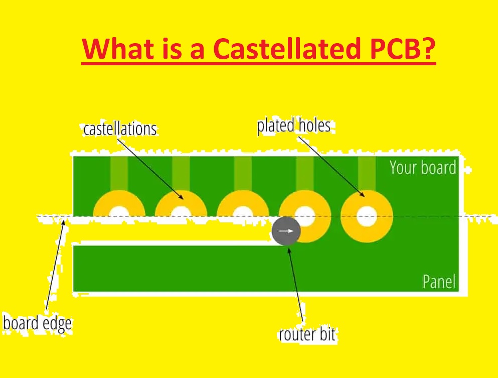
What is a Castellated PCB?
[adinserter block="3"]
A castellated PCB is PCB type that features plated edges on one or more sides. These plated edges normally come with a pattern of half-holes, resembling the battlements of a castle, so they are known as "castellated." These half-holes make easy soldering and mounting of the PCB board onto another board, making them best for applications like module integration or direct attachment to connectors.
Benefits of Castellated PCBs
Castellated PCBs have many advantages over traditional PCBs, which are
- Easy integration: The plated edges of castellated boards make simple the integration process with other boards or modules.
- Space-saving: By eliminating the use of separate connectors, castellated boards can save valuable space in electronic assemblies.
- Robust connections: The plated half-holes offer robust and reliable connections, make sure secure solder joints and mechanical strength.
- Design flexibility: Castellated boards provide different versatile placement options, helps designers to optimize space utilization, and accommodate certain application needs
Design Considerations
To design an accurate castellated PCB board, it is necessary to consider these parameters
Step 1: Determine the Purpose
Clearly define the purpose and needs of PCB. Consider factors like required application, size constraints, electrical features, and environmental conditions.
Step 2: Select the Appropriate Software
Select a reliable PCB design software that offers the necessary features for castellated PCB design. Commonly used software areAltium Designer, Eagle, and KiCad.
Step 3: Create the Schematic Design
Make a schematic design that captures the circuit functionality and connectivity. Make sure accurate labeling and documentation of components and connections.
Step 4: PCB Layout
[adinserter block="5"]
convert the schematic design into a physical layout. Carefully place the components, with consideration of power distribution, signal integrity, and thermal management. Follow the best techniques for trace routing and keep a balanced design.
Step 5: Define Castellations
Choose the locations and dimensions of the castellations on the board. Ensure accurate clearance between castellations and other components to prevent short circuits.
Step 6: Verify Design and Manufacture
Perform design rule checks (DRC) and electrical rule checks (ERC) to find and resolve potential faults. Make manufacturing files, like Gerber files, for manufacturing
Step 7: Assembly and Testing
Get services from reliable PCB manufacturers like JLCPCB to ensure accurate manufacturing and assembly of the castellated board. Perform thorough testing to validate the functionality and reliability of the final result
Troubleshooting Tips
While designing castellated boards, you can face some challenges. Here are a few troubleshooting tips explained to overcome common problems
- Make sure proper alignment and solderability of the castellations during the assembly process.
- Verify the compatibility of the castellated board with the target connectors or mating boards.
- Give attention to the mechanical strength and robustness of the castellated edges to handle any potential stress.
How are castellated pins created on PCB?
Castellated pins, also called castellations or half-holes, are made a PCB board during the manufacturing process. Here are some steps explained that show how castellated pins are created:
- PCB Design: In the PCB design phase, you define the shape and location of the castellated pins on the board's edge. These pins are typically located along one or more edges of the PCB.
- PCB Fabrication: Once the PCB design is completed, the manufacturer fabricates the PCB board according to design specifications. The castellated pins are made during the drilling and plating processes.
- Drilling: The manufacturer drills holes along the designated edge(s) of the board, where the castellated pins will be positioned. The size and shape of these holes are specified in the PCB board design files.
- Plating: After drilling, the holes are plated to offer electrical conductivity and structural integrity. The plating process comes with depositing a conductive material, like copper, in the drilled holes. This plating makes castellated pins.
- Separation: When plating is done, the PCB board undergoes a separation process. Where cutting the PCB along the designated edges s done to make individual boards. The separation process also cuts through the castellated pins, leaving them open and ready for the surface mounting process.
- Surface Mounting: The castellated pins are made to be soldered directly onto another PCB board or device. During assembly, the exposed castellated pins are aligned and soldered onto the required PCB or device. This design a secure electrical and mechanical connection between the two components.
Why should you choose castellated holes on Pcb?
- Surface mounting: Castellated holes PCB offers convenient techniques for surface mounting the board onto another PCB board or device. The exposed pins can be soldered directly onto the required component, removing the need for connectors or additional hardware.
- Space-saving: Castellated holes make the compact and space-saving design. They are useful in applications where space is limited or when have to get a low-profile connection between PCB boards or components.
- Simplified assembly: These holes simplify the assembly process by reducing the need for separate connectors or mounting hardware. This can reduce assembly time and expenses.
- Robust mechanical connection: Castellated holes offers a strong and reliable mechanical connection between the board and the component. The plated pins come with increased stability and durability than other surface-mounting techniques
- Electrical connectivity: The castellated pins also make a reliable electrical connection between the board and the components. They make a direct conductive path, ensure the proper signal transmission and reduce the chances of signal degradation or interference.
- Design flexibility: They also offer design flexibility, allowing you to make unique PCB board form factors and enable innovative product designs. We can position the castellated holes at certain locations on the board edge to fulfill our requirements.
- Cost-effective solution: By reducing the need for connectors or additional mounting hardware, castellated holes can help to eliminate overall manufacturing costs. The simple design and assembly processes, potentially provide a more cost-effective solution.
Castellated PCBs Manufacturing Techniques
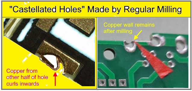
Manufacturing defects in metalized castellated holes, like the copper plating peeling and warping, have long been a problem in the production process. Castellated holes with copper burrs can cause physically and electrically unstable solder connections. It can also result in short circuits between neighboring pads in extreme circumstances.
Castellated holes are drilled and plated in the same way as standard PTHs, but the tricky part is getting the opposite half of each hole out without damaging the first or leaving extra copper behind.
Here detailed process for castellated holes PCB used JLCPCB explained
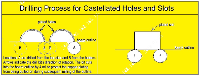
All of their drill and milling bits must approach the board from the proper side while rotating clockwise to make sure that any copper plating is always pressed against and never withdrawn from the backing wall. This ensures that the undesirable half of the copper ring is correctly and neatly cut off, leaving the other half intact. The JLCPCB's castellated process has reached a mature state of refinement. The current technique initially plates and drills the holes as it would for conventional PTHs, and then performs a 2nd drilling/milling pass to remove one-half from each hole while leaving the plating on the other half in situ.
Although this technique is more difficult than manufacturing ordinary PTHs, it was created to find that are accurate and pure. Castellated boards are more costly to produce due to the additional drilling process and the factor that they are often small and hence more difficult to handle.
Certain Requirements for Design
[adinserter block="6"]
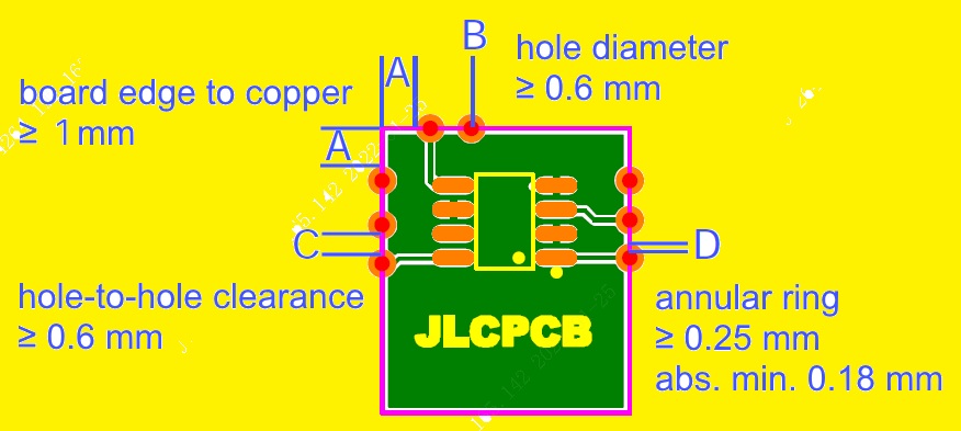
Basic Dimensions
| Dimension | Minimum |
| Board size | 10 mm × 10 mm |
| Board edge to castellated pad (A) | 1.0 mm |
| Castellated pad drill diameter (B) | 0.6 mm |
| Hole-to-hole clearance (C) | 0.6 mm |
| Annular ring (D) | 0.25 mm (absolute minimum 0.18 mm) |
Note: JLCPCB may extend annular rings that are less than 0.25 mm in diameter. Please provide a remark with your order if widths less than 0.25 mm are needed, and choose "confirm production files" to subsequently verify any modifications done.
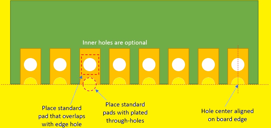
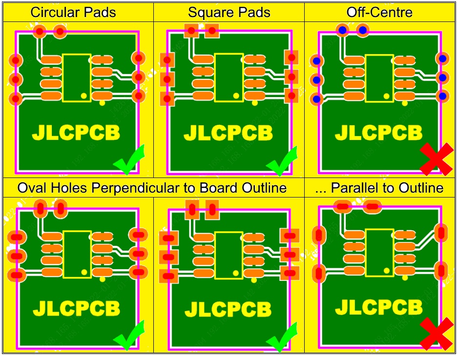
Pad Shape and Placement
Pads can be either round or rectangular. Only pads with long edges that are parallel to the board edge are permitted. Pads that are centered outside of the board edge are not allowed; they must be offset inward from the board edge.
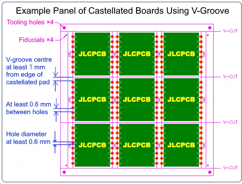
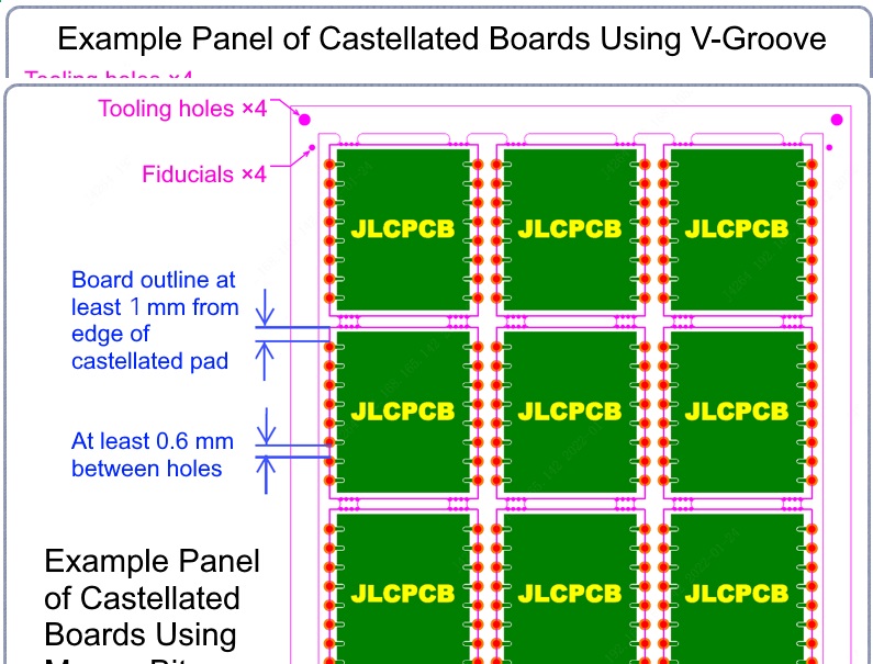
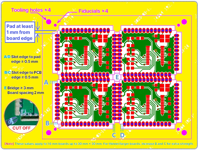
Panelising Castellated Boards
V-cuts or mouse bites can be used to penalize castellated boards. Notes that regardless of whether they are panelized, JLCPCB does not make castellated boards smaller than 10 mm by 10 mm.
If using V-cuts, note that the cutter damage castellated pads, hence cuts should only be made on non-castellated edges:
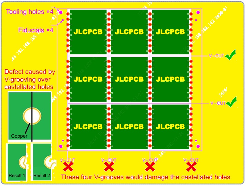
V-Cut Panels (Non-Castellated Edges Only)
Mouse Bite Panels
Boards with All Sides Castellated
[adinserter block="6"]
To realize your PCB ideas, high-quality PCBs are required. At JLCPCB, they are dedicated to upholding the highest manufacturing standards. To do this, they spend money on state-of-the-art machinery and work with reputable raw material suppliers from across the world. This supplier is able to minimize production costs brought on by large-scale impacts on manufacturing thanks to our five clever self-owned production bases, allowing us to provide our clients with accessible prospects for hardware innovation. Additionally, they give every new member up to $54 in registered coupons. Start purchasing premium PCBs by registering and uploading your Gerber files right now at https://jlcpcb.com.
Discussions
Become a Hackaday.io Member
Create an account to leave a comment. Already have an account? Log In.