 Dave Collins
The Problem:
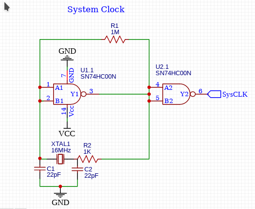
While debugging the HB6309 PCB REV1 I wanted to build a very stable oscillator I could drive the CPU and the Arduino with, I knocked together my standby: 1/2 of a 74HC00 and a 1K resistor and crystal with fairly mediocre results:
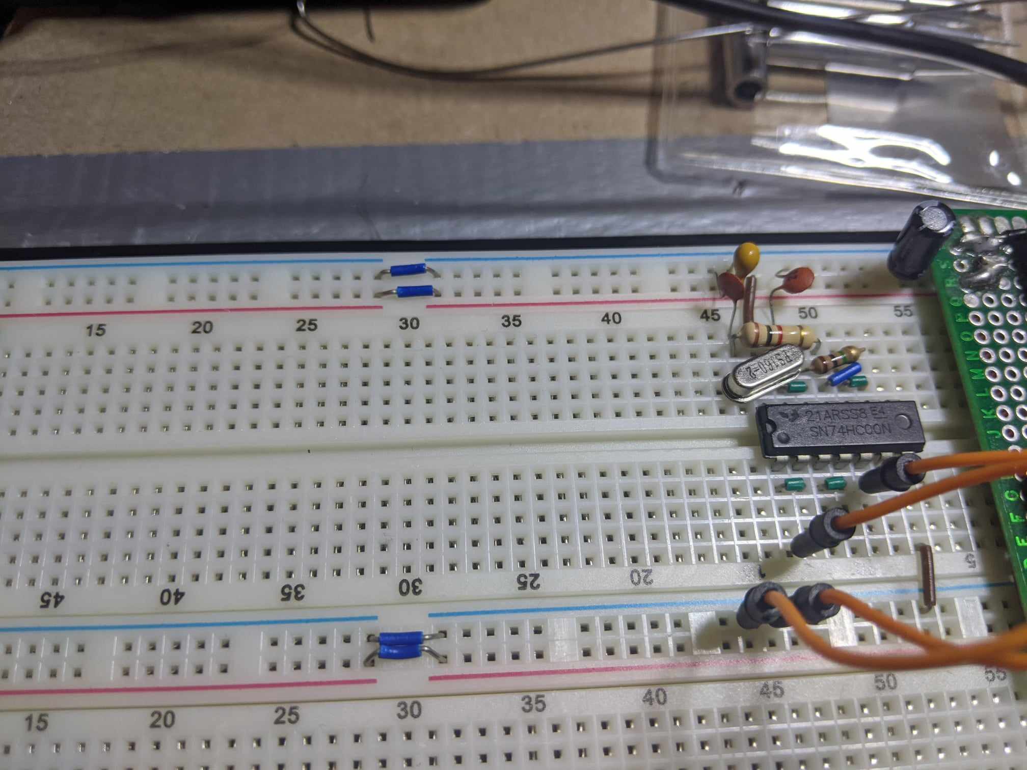 |  |  |
This is actually a very popular oscillator with hobbyists, and if were totally honest it works 90% of the time with no issues for the kinds of projects that we tend to gravitate towards. Even Grant Searle himself, uses the design in at least one of his Z80 builds. The biggest problem with this design (as you will see), is the inverter, a buffered NAND Gate, while its logical output is the same - its switching characteristics and internal circuitry are VERY different.
Before we get started, a gentle reminder to readers not familiar with my content. I am a hobbyist, and not a EE. I do have a very strong background in Civil Engineering in the telecommunications field, so if some of my examples or explanations are wrong - feel free to correct me! (we are all here to learn)
The issue:

The internals of the 74HC00, we see the buffered inputs, while insuring proper logical signal triggering, actually dampen the analog properties of the circuit. Additionally clamping diodes on the input (and output) of the inverter may play a roll as well, though certainly not nearly as much as introducing buffers to the circuit:
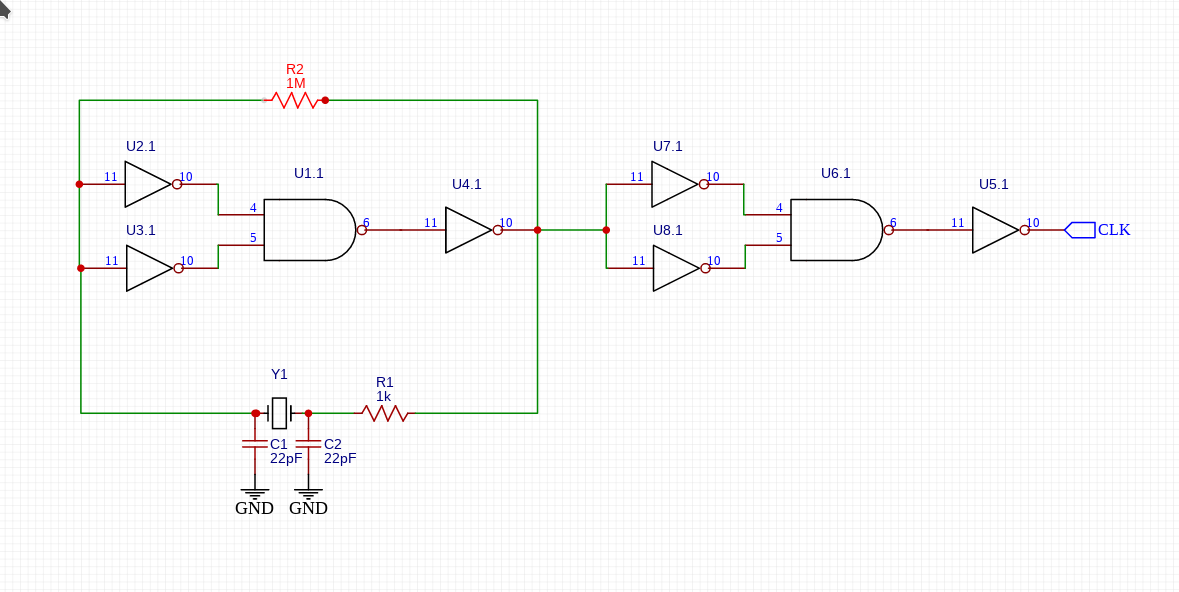
Just looking at the expanded circuit, you can see this is not even approaching a proper Pierce Oscillator. The root cause of the ringing are almost certain due to The first stage - to understand this better, lets look at a few different buffered inverters hooked up with a much better circuit recommended by Olin Lathrop on stack exchange
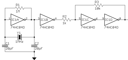
This circuit is considerably more suited to producing a very defined square wave. The first two buffers trigger the initial oscillation using a 1M Ohm resistor hooked in parallel. We see a sine wave (more or less, more on that in a second) on the input of 1A. A second inverter (1B) takes the trapezoidal output and cleans it up further. The second stage is a Schmidt Trigger, which introduces Hysteresis into the circuit, the first gate acts as sort of an amp to the second gate which drives the triangle wave produced by the first into a serviceable Square wave. Why not use just Schmidt triggers then?
Essentially, the first inverter is a linear amplifier - we know this because the 1M Ohm resistor from the input to the output acts as a bias to the input of the gate. This amplifier takes the relatively low sine wave output of the crystal, and turns it into a 5v PtP ish square wave. A Schmidt trigger is highly non linear (the whole point is to make the signals snap to the rails as happens in the second stage of the circuit), this is wonderful for generating a cleaner square wave than produced by 1B, but not so good as a linear amp.
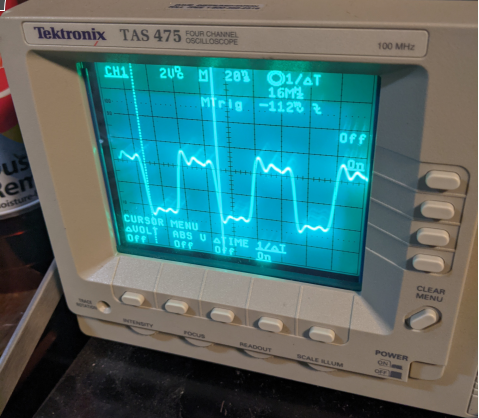
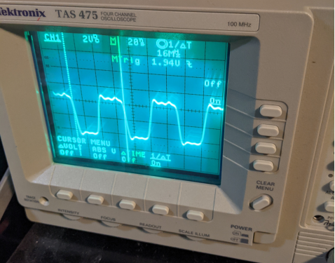
I got curious so I built the circuit with a 74HC14:

This is the input of the first gate, see how the signal here is very non-linear, also note the fringing around the edges; on a digital scope this would be rolling like crazy as the time base changes, additionally the amplitude fluctuates as well -- this would be a wonderful circuit to analyze on a spectrum analyzer (unfortunately for me I only have access to that at work, and certainly not in a format I can probe a simple circuit I built at home)
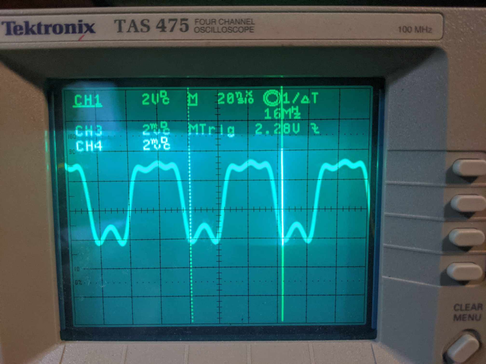
The output IS technically a VERY defined square wave, but the time base is severely effected by the multiple triggers, interfering as the time base shifts:

Then I tried the 74HC04:
I kind of knew the results would be fairly similar to the simple 1/2 NAND solution:
Basically - this is the same though the multiple inverters pronounce the ringing on the High level base instead of the low level base. (this is also with a small value approx 33 Ohm dampening resistor on the output for good measure!) The results a very similar with a buffered gate, and it all goes back to the linear amp:
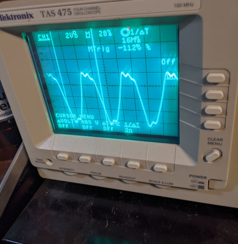
The additional buffers, make it much more difficult to bias the input of the first inverter, in short the passive analog properties of the circuit are dampened because of the input and output stage of the package. additionally, the input swings way past zero -- almost -1V definitely not what we want! What if we try a inverter that is completely unbuffered? A pin compatible package is available in the 74HCU04.
74HCU04:
The datasheet specifically has application notes for doing exactly what we are trying to do here, if that's not evidence enough lets check it out on the analog scope:
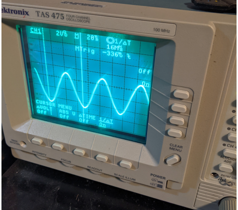
See how essentially, the input is a perfect linear sine wave? Starting with a clean input wave we end up with much more serviceable results on the output:
Further tweaking could clean up the duty cycle - but this is fairly close to what I was looking for! A very nice, well defined square wave with little ringing (if any -- I am using a solder tail to pull a ground off of the board and my probes are not the best but definitely not the worst).
Conclusion:
Thanks for taking the time to share this journey with me! If you hadn't had a chance to check out my current project on Hackaday.io, I am working on a uATX 63C09 / AVR Multiprocessor system, If you're interested in that sort of thing. Feel free to comment where I got some of the engineering theory here wrong, as I am sure there's tons that could be clarified or corrected.
Discussions
Become a Hackaday.io Member
Create an account to leave a comment. Already have an account? Log In.