 Dave Collins
 Yann Guidon / YGDES
-
New DC-DC Circuit for the 48k Speccy
3 days ago • 0 comments
Just before applying the DC-DC mods for the original circuit I received this 48K spectrum from a friend, in a mostly working state. It needed to have the membrane replaced as well as one of the 32K ram chips. Through the process of rework the DC-DC converter circuit began to fail. I believe as a result of being run at a high level for a long period of time, from an unregulated 9v supply that may have drifted slightly.
On initial inspection, I determined the 4116's must have failed as TR4 / TR5 kept blowing. I replaced them (t4 and t5) and removed the ram chips, to no avail as the transistors kept failing even with the ram chips removed. The next on the list to check was all the capacitors, I verified none were open or dead short with good ESR values ( all electrolytic were replaced first thing - and the board worked for a few hours at least). I suspected the coil was bad. At this point I started to deep dive into the circuit and read through two separate circuit descriptions trying to determine:
- why this circuit fails so much.
- why this was the most modified part of the circuit throughout the revisions.
- can this be improved uppon.
I asked my father, who was an EE from the 60's all the way to the 90's to take a look at the inverter / DC-DC circuits across the several revisions as he's vastly better at looking at analog circuits than I am. Together we determined that the DC-DC mods specifically address regulation and clamping issues in the previous versions of the circuit. While these improve supply output and manage transient voltages which feed sensitive ram chips it does not address what is conspicuously missing from ALL revisions of the 48k DC-DC circuit; 4116 bring up timing.
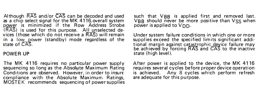
The 4116's and by in large the transistors inside the DC-DC circuit fail because the supply does not adhere to this note in the 4116 Datasheet:
![]()
Simply put - There is no timing mechanism beyond the R/C delay inside the circuit itself, which grants exclusively that VBB (-5v) is applied first, and removed last. Furthermore, when power is removed to turn off the system if the ground path is eliminated by disconnecting the cord completely or isolating the ground line in an improperly wired switch. There is no way to assure any sort of state on power down.
So - specifically when the 4116's fail, and they usually will, the DC-DC circuit is often damaged by an over current condition on the digital 12v rail.
So how did I improve upon the design:Back in the 80's the most commonly used dc power supply was an unregulated 9v center negative power supply. Specifically because of this utility its obvious to me that that is the reason that iconically thrifty Sir Clive and his engineers chose this to be the supply they were to use. Moreover - not wanting to spend any amount on a switch for every unit allowed them to cut the prices even further to save Sinclair millions, by simply having the public unplug the thing or turn the switch off at the wall socket. What was needed was a minimal, cheep and dirty power circuit to create the multiple rails required for the computer and not break the bank. I think they did the best they could with the limits they had, and specifically the computers worked well enough in the day for this oversight to not matter nearly as much as it does today.
Today, we have commonplace, high quality 12V regulated power supplies that run cool and efficient and don't really break the bank. I decided to remove the DC-DC circuit in my issue 3, and use an external regulated center negative 12v power supply to power the whole computer.
This has several advantages:
- The supply is more efficient - we no longer have to "boost convert" a 12v rail using a charge pump and inverter. This reduces losses to multiple conversions going from 9v - > +5V -> +12v & -5v
- The supply is cooler - the LM7805 linear positive voltage regulator gets...
-
HB63C09 Mezzanine Connection
01/21/2024 at 02:31 • 0 commentsThe mezzanine, your gateway to off board IO
Going over the memory map from the REV3 board, the astute will notice the entire IO range selects the AVR request grant logic. This poses an issue for off board requests from the mezzanine connection. To resolve this, the XSIN (transceiver inhibit) signal is utilized. XSIN is a active high signal (for now) that cuts off the bus transceiver output enable pin. This in effect leaves the bus available to the mezzanine connection:
![]()
When the loop starts inside the firmware the AVR (an ATMEGA32E micro controller) is just poling for IO requests. When it catches one, the MRDY state is already asserted on the CPU and the buses and the E and Q pulses stop in the state that they were in. This includes the data bus, r//w line and the address bus (along with all the other control signals as well). Immediately following this, it reads the XSIN line and determines if it is high. If so the IOGNT_ signal is immediately sent to the request/grant circuit and the read / write cycle can continue. This does have the disadvantage of added delay and a momentary clock stretch on every IO request, however it is very short, only a few cycles of the system clock. This was a needed trade of to keep the selection logic as simple as possible without expanding to a higher chip count.
In order to use the mezzanine expansion connector, the IO request logic must be replicated on the expansion. The IO request must also be assigned to an unused address in the IO range (for example, any address in A010-AFFF). The selection signal must be active high and linked to the XSIN line, which means that a standard address decoder must either have active high outputs or be inverted before using the signal. The XSIN pin is an input on the AVR, and it is pulled low by a 10k resistor. Only one output on the expansion should select this pin, because the logic on this line is push pull and multiple signals driving the pin high could cause a short circuit. During reset the AVR pulls this line high to zero the bank register. Currently I can not test the mezzanine until I resolve the potential short circuit. This is likely to change to simply having the reset pin for the register driven by RES (inverted RES_, which is generated by the reset circuit) but it was not high on the list of things to work out in this board revision, and so it was omitted. I am also considering changing the functionality of the pin XSIN to active low, by building out logic. Since the actual scope of the signal is for only one device it makes better sense to not make this a priority over other things which could potentially take more board space. The advantage to this is all of the signals going into XSIN could be open collector outputs and this would drastically increase the usefulness of the signal in a multi-slot expansion set up, if for instance somebody were to build a breakout with multiple slots.
If you'd like to learn more about the HB63C09M follow this link to the main project page.
-
7404/14 - Not all inverters are the same.
10/28/2023 at 04:21 • 0 commentsThe Problem:
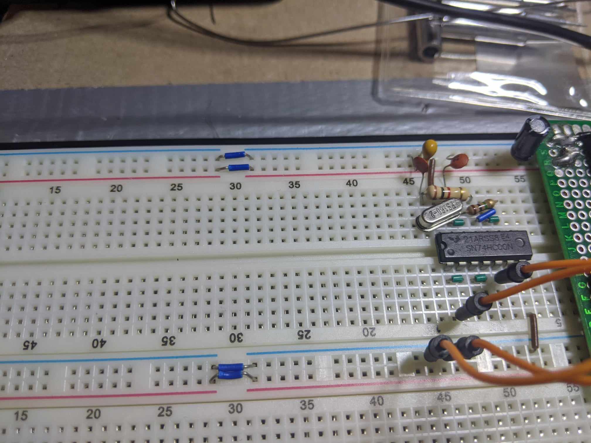
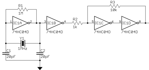
While debugging the HB6309 PCB REV1 I wanted to build a very stable oscillator I could drive the CPU and the Arduino with, I knocked together my standby: 1/2 of a 74HC00 and a 1K resistor and crystal with fairly mediocre results:
![]()
![]()
![]()
This is actually a very popular oscillator with hobbyists, and if were totally honest it works 90% of the time with no issues for the kinds of projects that we tend to gravitate towards. Even Grant Searle himself, uses the design in at least one of his Z80 builds. The biggest problem with this design (as you will see), is the inverter, a buffered NAND Gate, while its logical output is the same - its switching characteristics and internal circuitry are VERY different.
Before we get started, a gentle reminder to readers not familiar with my content. I am a hobbyist, and not a EE. I do have a very strong background in Civil Engineering in the telecommunications field, so if some of my examples or explanations are wrong - feel free to correct me! (we are all here to learn)
The issue:![]()
The internals of the 74HC00, we see the buffered inputs, while insuring proper logical signal triggering, actually dampen the analog properties of the circuit. Additionally clamping diodes on the input (and output) of the inverter may play a roll as well, though certainly not nearly as much as introducing buffers to the circuit:
![]()
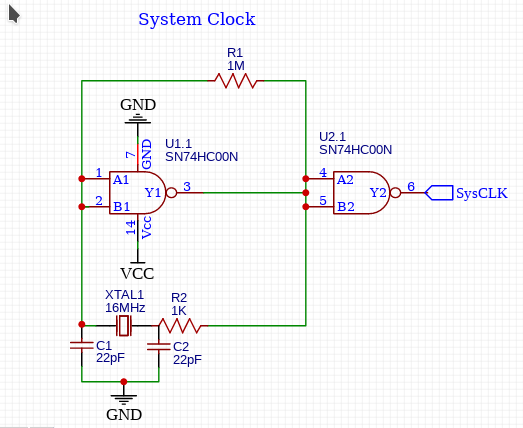
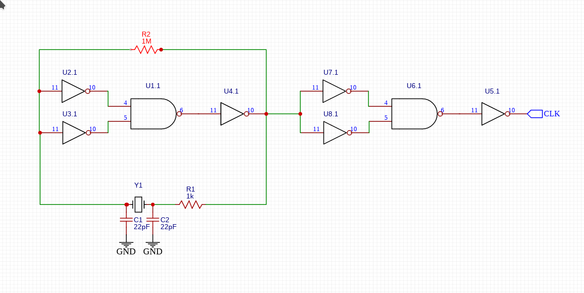
Just looking at the expanded circuit, you can see this is not even approaching a proper Pierce Oscillator. The root cause of the ringing are almost certain due to The first stage - to understand this better, lets look at a few different buffered inverters hooked up with a much better circuit recommended by Olin Lathrop on stack exchange
![]()
This circuit is considerably more suited to producing a very defined square wave. The first two buffers trigger the initial oscillation using a 1M Ohm resistor hooked in parallel. We see a sine wave (more or less, more on that in a second) on the input of 1A. A second inverter (1B) takes the trapezoidal output and cleans it up further. The second stage is a Schmidt Trigger, which introduces Hysteresis into the circuit, the first gate acts as sort of an amp to the second gate which drives the triangle wave produced by the first into a serviceable Square wave. Why not use just Schmidt triggers then?
Essentially, the first inverter is a linear amplifier - we know this because the 1M Ohm resistor from the input to the output acts as a bias to the input of the gate. This amplifier takes the relatively low sine wave output of the crystal, and turns it into a 5v PtP ish square wave. A Schmidt trigger is highly non linear (the whole point is to make the signals snap to the rails as happens in the second stage of the circuit), this is wonderful for generating a cleaner square wave than produced by 1B, but not so good as a linear amp.
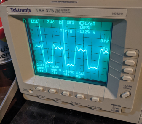
I got curious so I built the circuit with a 74HC14:
![]()
This is the input of the first gate, see how the signal here is very non-linear, also note the fringing around the edges; on a digital scope this would be rolling like crazy as the time base changes, additionally the amplitude fluctuates as well -- this would be a wonderful circuit to analyze on a spectrum analyzer (unfortunately for me I only have access to that at work, and certainly not in a format I can probe a simple circuit I built at home)
The output IS technically a VERY defined square wave, but the time base is severely effected by the multiple triggers, interfering as the time base shifts:
![]()
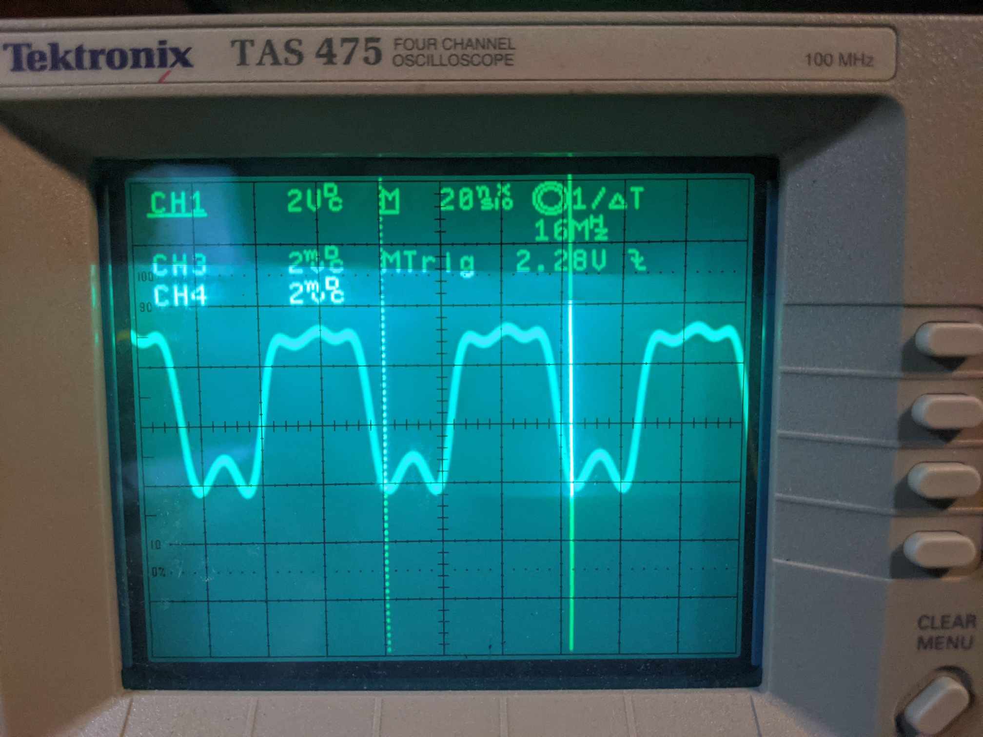
Then I tried the 74HC04:
I kind of knew the results would be fairly similar to the simple 1/2 NAND solution:
![]()
Basically - this is the same though the multiple inverters pronounce the ringing on the High level base instead of the low level base. (this is also with a small value approx 33 Ohm dampening resistor on the output...
Read more »


 Lutetium
 esben rossel
 David Davenne
 Robert Hart
 Stefan Wagner
 jareklupinski
 Lasith Ishan
 Ahmed Azouz
 John Opsahl