 AVR
AVRood news today!!! The SunLeaf PCB is pretty much finished and is being put through the preparations to be fabricated at OSHPark and then hand assembled by me soon after ! The truth is the SunLeaf board has been done for a few weeks but it wasn't near ready for ordering, since then components have been shifted around and libraries cleaned up, and now its ready! After a bit more last minute discussion amongst the design team the design will be locked and fabrication files will be published at the time we order.
So without further ado here is the 0.1 Alpha SunLeaf Hardware
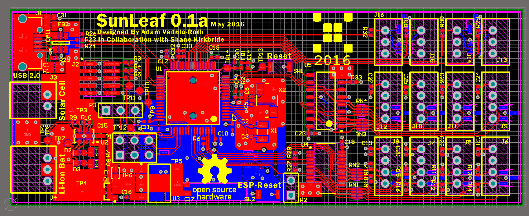
Overall the specifications of the 0.1 Alpha prototype design reflect the ones initially defined, but there were some changes in the schematic. The changes in the schematic included the addition of 4 analog inputs, additional ESD protection (ports/USB), MCU schematic revised from reference, test points for oscilloscope, alligator test point pad, and jumpers for the ESP UART. The alligator test point is something special I came up with, often times it can be difficult to hook up a scope if there isn't anything to clip the alligator clip to, so I devised a test point footprint specifically for this purpose. The pad is rectangular with rounded corners and appears on the top and bottom of the board:

I haven't seen anyone else do this before, so I thought I'd give it a try and see how it works out, feel free to try it yourselves.
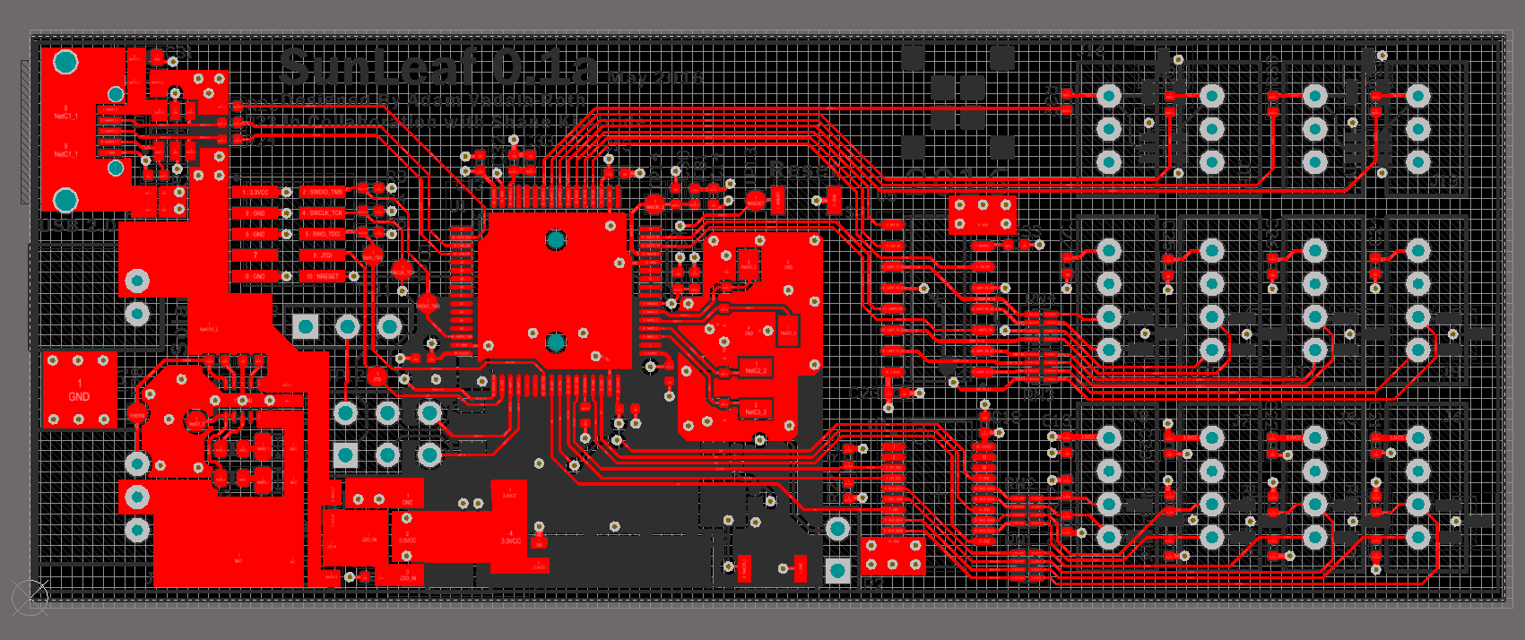
So PCB topology. SunLeaf is a 4 layer PCB, the two outermost layers are signal and component mounting layers, the two internal layers serve as a ground plane and a 3V3 DC power plane respectively. Most of the components and system are placed on the top side of the PCB, also 90% of all signals are routed on the top layer. Some components are placed on the bottom side of the PCB, mostly ESD protection on the ports and the entire ESP8266 ESP-02 system-on-module. The ESP module is bottom mounted to keep the PCB size down. Due to the layer stackup being Top>Ground>Power>Bottom there is some concern for interference with the ESP-02 system-on-module so there is a ground pour placed beneath it carefully stitched to the internal ground plane.
SunLeaf PCB Layers and Topology:
Top Layer - Signals and Component Mounting
Internal Plane 1 - GND Plane
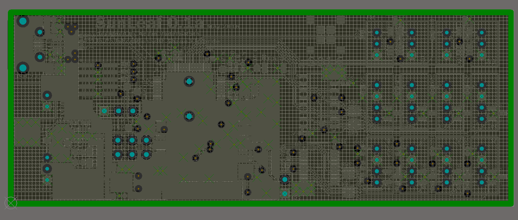
Internal Plane 2 - Power Plane
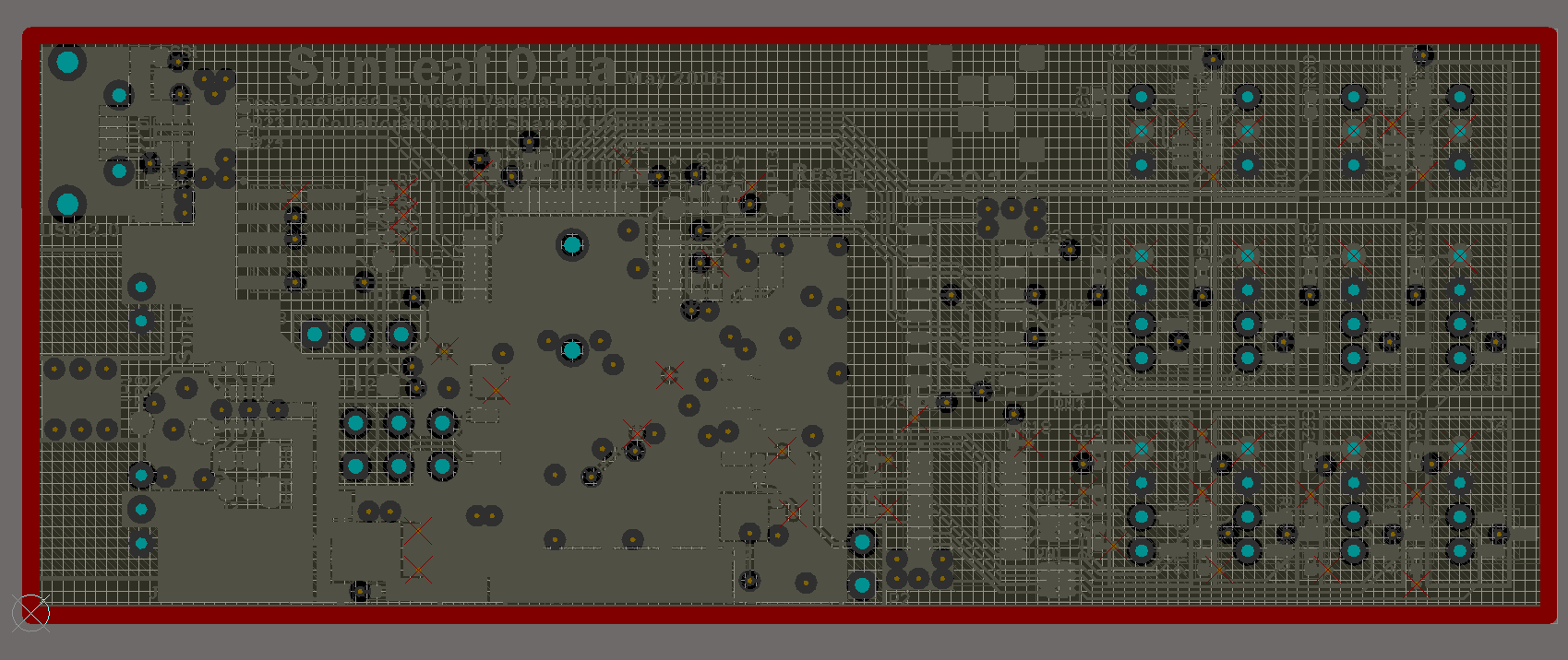
Botom Layer - ESD and ESP Mounting

So thats really all there is with the PCB! Updated schematic and sources can be found in the links on the side of the project page. A bit more review with the team and SunLeaf will be out to OSHPark soon, stay tuned for more updates!
Discussions
Become a Hackaday.io Member
Create an account to leave a comment. Already have an account? Log In.
thanks a ton!!! I've been taking my time with this one doing every step the best I can, I'm really excited to get it off to the fab and see how it turns out!
Are you sure? yes | no
Awesome work, I'm looking forward to seeing future updates!
Are you sure? yes | no