After a long time spend testing and thinking about the right solution to all the problems, I have made multiple alterations to the current prototype. Some of them require a different design, so the new board including these signal processing units should be produced soon.
Noise figures
Almost all of the simulations I performed in LTspice were noiseless. The output signals were neat and easy to process. To consider a more real case I added a white noise signal to the output of the preamplifier so that it resembles 60keV pulses. After picking the right values I ended up with pretty dense noise of 8 mVpp and exponentially falling pulses of amplitude 2.5mV below noise floor. Such subtle changes rendered the old simulation completely useless. The old smooth signal was replaced with spiky and indistinguishable fluctuations. In the old version of the circuitry you could easily see that the peak value was repeatable, now it will be a lot harder.
Updated approach to signal processing
Because of all that noise present in the signal I had to redesign the whole signal path. It will no longer have any subtractors or rectifiers which would have to be set individually. Instead there will be some new blocks, which will help to extract and measure the peak from the ever-present noise. Here is a detailed schematic:
- Starting from the left the preamplifier feeds the signal to an inverting amplifier which is a preset subtractor. It reduces the DC of the signal close to 0V by subtracting the operating point of the amplifier which is about 2.45-2.50V. By this treatment the signal is ready for further processing without any undershoot that would be caused by capacitive coupling if we chose to use a capacitor to cancel the DC.
- Next functional block is 4th stage Bessel low-pass filter implemented using Sallen-Key topology. The gain of the whole filter block is set to 50V/V and the corner frequency to about 100kHz. Its aim is to reduce the high frequency noise and shape the pulses so that they resemble gaussian ones. The delay and overshoot are crucial for this application as well as variable gain that can be suited to application. Because of these reasons Bessel type and Sallen-Key topology is used. To design these filters, I used online calculators available from Analog Devices and Texas Instruments.
Notice that after the first stage the signal is fed to the comparator segment for further processing. It is necessary for the comparators to work with quickly shaped signal without huge distortions in order to give reliable results concerning pulse duration and its rising slope before it is properly shaped and prolonged.
![]()
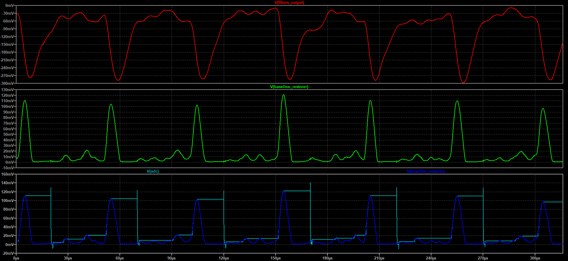
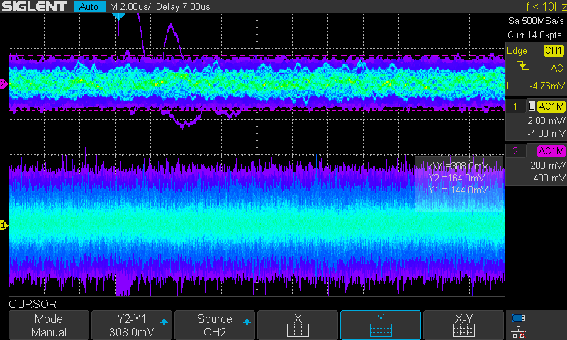
Pulse shaping by filters
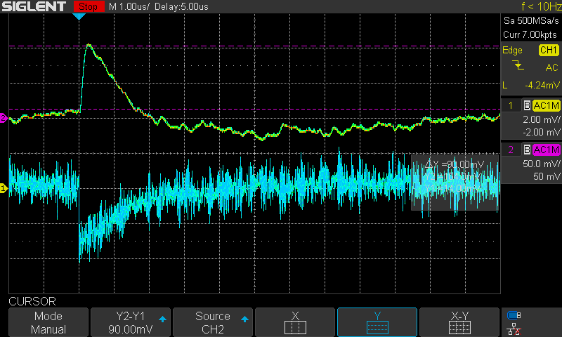
- From the filters the signal is fed onto the baseline restorer which function is quite peculiar. Baseline restorer recreates input pulses removing any undershoot from the signal and providing pulse output height in response to the input signal level difference. With a proper baseline restorer any subtractors become obsolete and high dose rates can be handled without any errors caused by a temporary baseline shift.
- The finishing stage of the signal path is a fast peak detector with reset. This time it is based on common amplifiers. Despite the fact it is fast and accurate. Its topology is extended to prevent capacitor discharge through rectifying diodes. Another addition is a digital switch serving as a reset, which will be triggered by MCU.
![]()
Baseline restorer and peak detector signals
Below the analog signal processing path is the semi-digital segment responsible for pulse detection:
- The signal from the fast filter is AC coupled and inverted so that comparators can work with positive pulse without any DC. The undershoot does not play any significant role in this segment, because the amplitude is not that important as long as it is above a certain level. This buffer block is not absolutely necessary, but it was placed to meet an even number of operational amplifiers in the design.
- Conditioned signal is later supplied to a non-inverting comparator with hysteresis that acts as pulse duration indicator.
- Before the second comparator input a differentiator block is placed. It is adjusted to quickly go into negative saturation as soon as a rising slope is detected. Following this differentiator block is an inverting comparator with hysteresis, which translates the analog op amp signals into digital states, indicating rising slope.
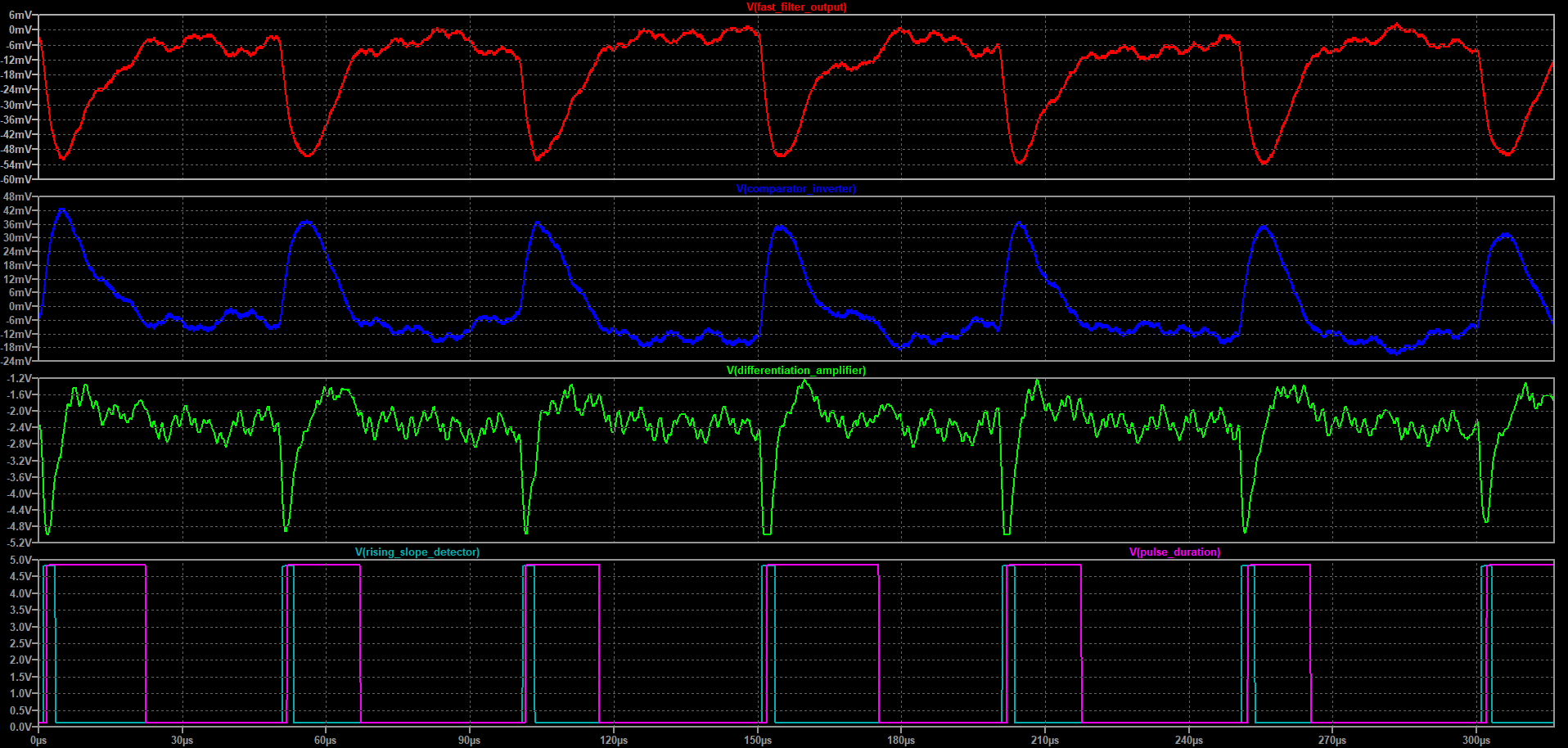
This double comparator block job is to detect pile up and send trigger signal to the MCU. If there appear at least two rising slope pulses while pulse duration is still triggered the MCU will not measure such pulse, as its height certainly was affected by occurring pileup. The exact values of components in the third prototype have to be yet properly calculated and checked. Voltage sources present in the simulation are for ease of altering the parameters and will be replaced by voltage dividers stabilized with a capacitor in the practial design
Detector resolution with noise
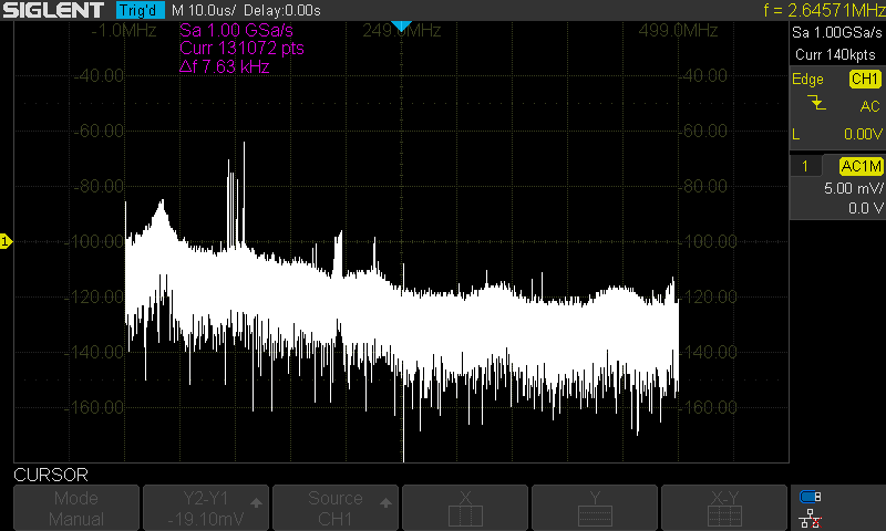
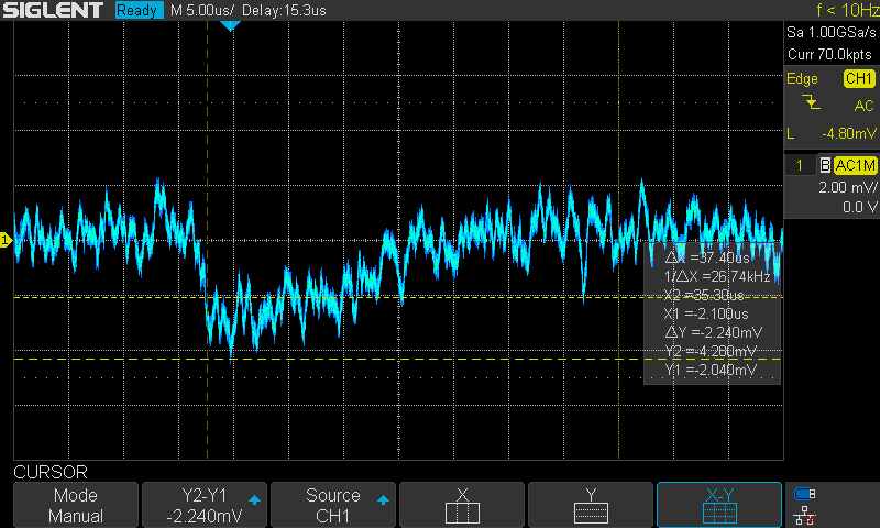
Observing the output signals that will be later sampled by an ADC it is easy to notice that even the same energy signals end up represented by different voltage levels. It is due to significant noise amplitude that affects the actual peak value. Even with the low-pass filters the fluctuations in the signal remain and error is still present. This causes the spectrum of certain energy to be spread and not visible as a single bar in the graph. The main source of the noise are PIN diodes and the preamplifier. By changing the detector to a photomultiplier tube with scintillator I might be able to improve the resolution, but that Is yet to be tested. Currently the circuitry of the detector will be tuned to minimize the noise impact on the pulse readout, having in mind that semiconductor detectors have their limits.
One way to minimize the distortion in the pulse is to increase the feedback resistance in order to extend the pulse duration and eliminate the high domain frequencies using a low-pass filter. It proves itself effective as far as simulation is concerned. On the one hand it reduces the amplitude spread and noise distortion, but on the other increases dead time of the detector.
The detector is also extremely sensitive to electromagnetic interference and RF signal coming from the radio stations and BTS. Radiation pulses are in low frequency domain and in order to measure them without greater distortions a low pass filter is absolutely crucial.
Preamplifier with LMP7721 test
To check if a lower GBW and lower noise operational amplifier would improve the TIA stage I performed a few tests with LM7721. The presets were similar to the 1 diode tests with bootstrap and LTC6268. The noise frequency was lower due to the bandwidth limitation as LMP7721 GBW is only 17MHz. The overall amplitude of the pulse was about 2-2.5mV below noise floor which was quite the same in comparison to LTC6268. The parameters have not changed in any favorable way. The TIA design will remain with LTC6268.
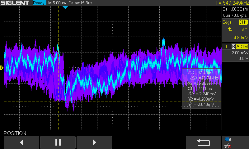
Triple amplifier tests
To verify how simple amplification affects noisy signal I mounted amplifiers in the prototype and set overall gain to about 250V/V. From the screens taken you might see that the dense noise is not amplified because of the limited GBW of used amplifier (LT6232). Furthermore, there is an undershoot visible as amplifiers are connected through a capacitor. On the whole, even common amplifiers provide some kind of filtering that removes the high frequency noise. Sometimes the simulation in LTspice may provide too ideal data, and signals resembled without including the imperfections of the components, design, amplifiers or parasitic effects. I hope that some imperfections may actually improve the signal to noise ratio, but that will be verified in the third detector design.

Discussions
Become a Hackaday.io Member
Create an account to leave a comment. Already have an account? Log In.