Time to fully disclose the operation of the CPU ! The complete schematics can be found in the files section, SQ1C1841.PDF.
REGISTER B
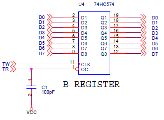
Let's start with the simplest part. Since the CPU has no ALU, the most important task of the CPU is moving data from one place to another. So in one cycle it fetches a byte from memory and stores it in the B register. In the next cycle, it can put the contents of the B register on the databus and store the value somewhere. So the B register can be loaded from the databus (at the end of a low pulse on TW), and its contents can be placed on the databus (when TR is low).
The signals are called TR (T-Read) and TW (T-Write) because the B register was previously named "Temp".
In the decoder part you will see that the write and read signals come almost at the same time. It was expected that at the end of these signals, the databus would keep its last signals for perhaps twenty nanoseconds after the '574 was tri-stated at the end of the TR signal. But this did not work, so the TR signal had to be delayed by a small 100pF capacitor. This capacitor was not on the first version of the board. It is also not on the NAC pcb, it must be added on the NAC as a modification.
Note that the low side of the capacitor is connected to VCC (5 volt) instead of ground, this is because it was impossible to make this connection to ground with a trace on the pcb. But it was possible to connect it to VCC, so that was chosen. It makes no difference for the operation of the capacitor.
ADDRESS GENERATION
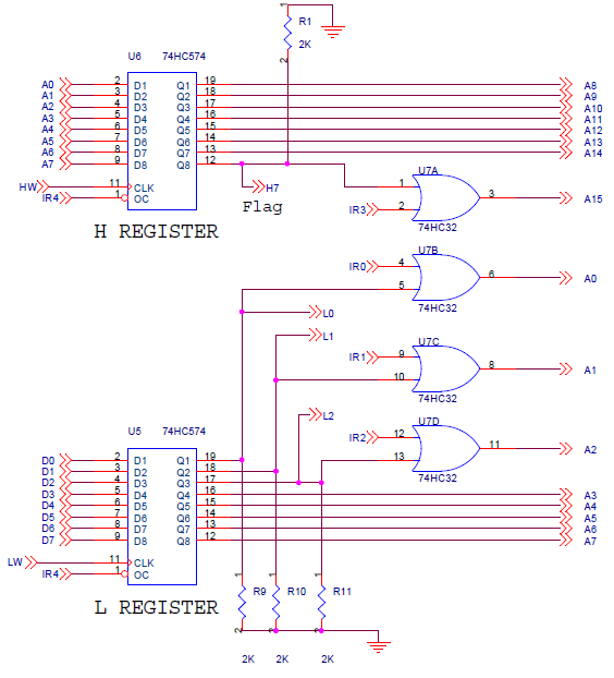
The L register can be written directly from the databus by making LW low. The output of the L register generates the address bits A0 - A7. Note that the lowest 3 bits are OR'ed (with HC32 gates) with the microcode bits IR0 - IR2. In most cases, only IR0 is used (when the H and L outputs are active), to select either LSB from the address in HL, or select the MSB from (HL+1).
The H register can not be loaded from the databus. A value must first be in the L register, that will generate the address bits A0-A7, and then these address bits can be loaded into the H register by making HW low. The output of the H register generates the address bits A8 - A15. Note that the highest bit of the H register is called "Flag". This is connected to one of the address inputs of the microprogram storage, and makes conditional jumps possible.
An important feature is, that the outputs of the H and L register can be switched off (tri-stated) by the microcode bit IR4 (at pin 1 of the '574 registers). The outputs have pulldown resistors to pull the lines to zero in this case. (For A3 - A14 the pulldown resistors are external to the cpu). Now, by using the microcode bits IR0 - IR3, the microcode can generate 16 fixed addresses: A range in RAM (0x0000-0x0007), used for addressing the "software-registers" A, PC and SP, and a range in flash ROM (0x8000 - 0x8007) used to access constants for loading the pc at startup, and to access constants for jump addresses in microcode.
The fact that H and L can be loaded independently of each other makes it easy to manipulate tables of 256 bytes, like the stack area, the increment and decrement tables, and the area used for the CMPB instruction.
MICROPROGRAM
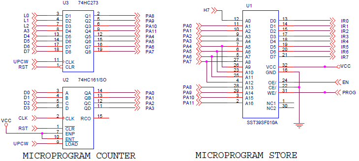
There are two parts (U2 and U3) that together produce the 12-bit microcode address. Only the lowest four bits are in a '161 counter chip and actually count (at each cpu CLK pulse). That means that a stretch of 16 micro-instructions must always end with a jump to another position in the microcode (otherwise the same 16 micro-instructions will be repeated).
The microcode address is connected to the address bus of the Flash ROM chip U1, together with the flag bit this makes 13 address lines. So why are the unused address lines (A9 -A12) not simply connected to logic 0 (GND) ? That is because we also want to be able to program the Flash chip while it is soldered in the CPU. For programming it, we need to present a certain sequence of commands to the chip, as mentioned in the datasheet:
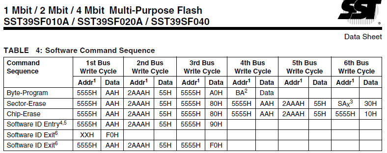
We see that the address must be alternated between 0x5555 and 0x2AAA in order to program bytes or to erase the chip. By connecting A9 - A12 to A5 - A8, as shown above, it is possible to generate these addresses although only 13 address bits are actually used.
At the right side of the Flash chip you see that it delivers the eight microcode bits IR0 - IR7. It also shows the two signals EN and PROG, that are connected to pins of the CPU to enable flash programming (but on the CLOCK pcb, EN is called US_OE, and PROG is called US_WR).
The shown connection of the Flash chip is the way it was connected on the NAC pcb and on the first version of the 1x1" cpu. However, the TSOP version has another pinout than the DIP version, and the cpu pcb had to be redesigned with a correct flash pinout. The flash had to be turned 180 degrees, and it was impossible to connect all traces again. Therefore, the connection of the address bus was changed a little:
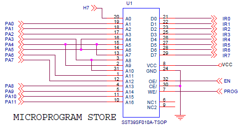
Address connection looks a bit messy but the effect is the same. In the following screenshot you can see how flash pins 13 - 16 are connected to alternate signals :

MICRO-INSTRUCTION DECODE
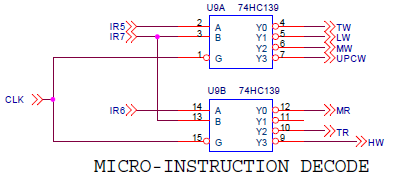
This decoder determines the data routing for each cycle.
The lower HC139 half will select which device can place it's contents on the databus. There are only two: MR (memory-read) will let the external memory (or input port) place something on the bus (From which address that information comes is decided by the address generation circuit, discussed above). The TR (Temp-read) will let the B register place its contents on the databus. The HW (H-register-write) signal is also on the lower multiplexer but this will load the H register from the lower address bus (described in address generation). The upper multiplexer might have been a better place to connect the HW signal, but that was full.
The upper HC139 will select which device is written:
- TW will write the databus contents to the B register
- LW will write the databus contents to the L register
- MW will write the databus contents to external memory (or output port)
- UPCW will write the B register and the upper four bits of the L register to the micro-program counter. The current microcode version uses only 256 addresses, the bits loaded from the L register are always 0 (the output of L can be forced to 0 by making IR4 high).
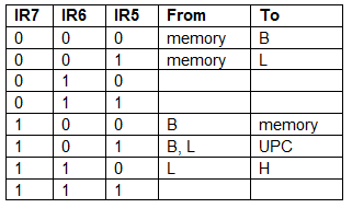
The decoder gives us the following routing options, based on the values of IR5, IR6 and IR7:
CPU EXTERNAL CONNECTIONS
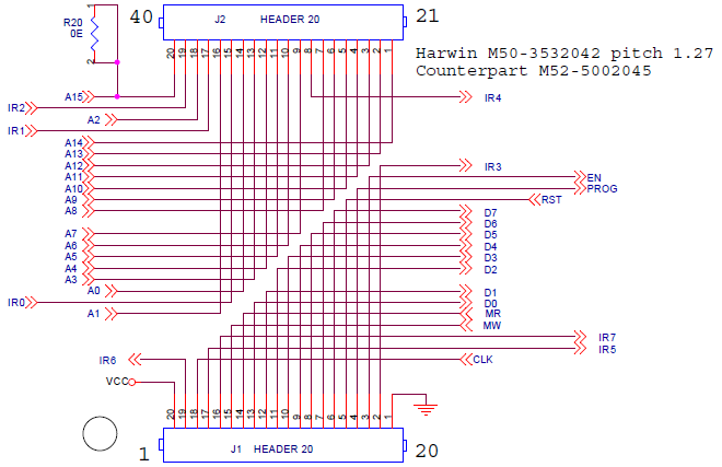
This last part of the schematic show the connections to the outside world. Pins 1 and 40 are not actually connected on the pcb, a little wire is needed (as explained in THIS log). If you have read all previous logs, there will be no surprises here. Not shown on any of these schematic sections is that there are also 4 decoupling capacitors on the pcb.
This is the end of the grand tour through the little CPU !
Discussions
Become a Hackaday.io Member
Create an account to leave a comment. Already have an account? Log In.