This project is very much a race against the clock. The idea for this project occurred to me after the first week of september, leaving three weeks before the end of the Square Inch Contest. Since it involves processor architecture, hardware and pcb design, and software, this is hardly possible in three weeks when you also have a job.
The project was not finished in time for the square inch deadline, perhaps the Hackaday prize 2019 will bring more luck.
Well let's start with the usual characteristics:
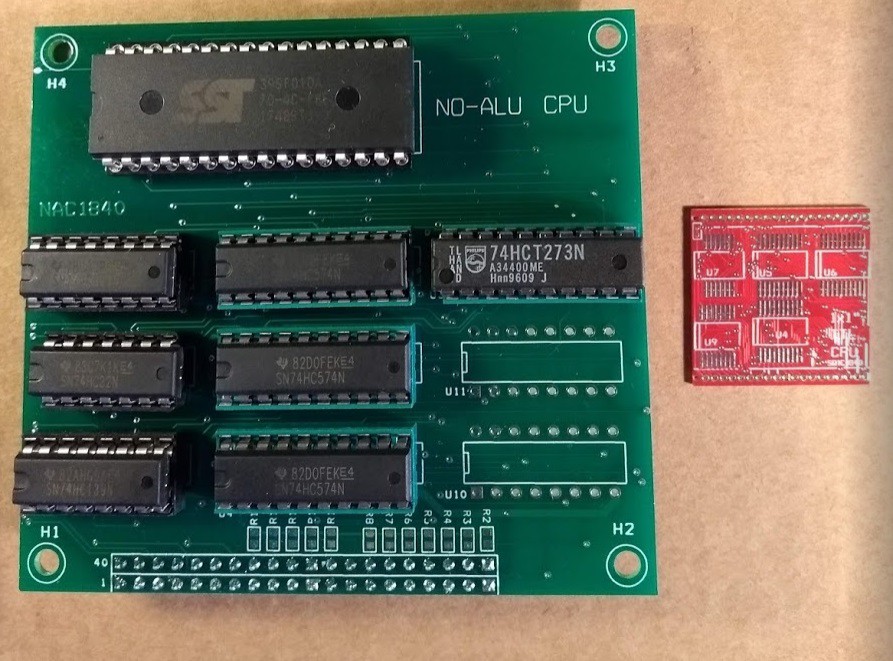
HARDWARE FEATURES
- 8 data lines
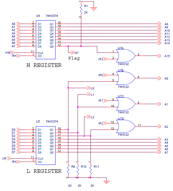
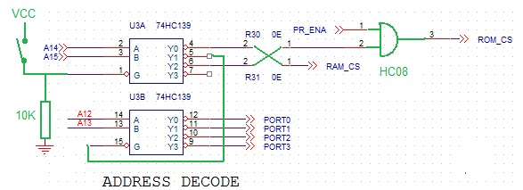
- 16 address lines
- Single 64kB memory space for program and data
- Memory Read and Memory Write lines
- Reset and clock inputs
- 5 volt power lines
SOFTWARE FEATURES
- Zero page addressing
- Indirect Zero Page addressing
- Immediate addressing
- Load, store and compare instructions
- Stack
- Conditional branches
- Subroutine calls
- Memory-mapped I/O
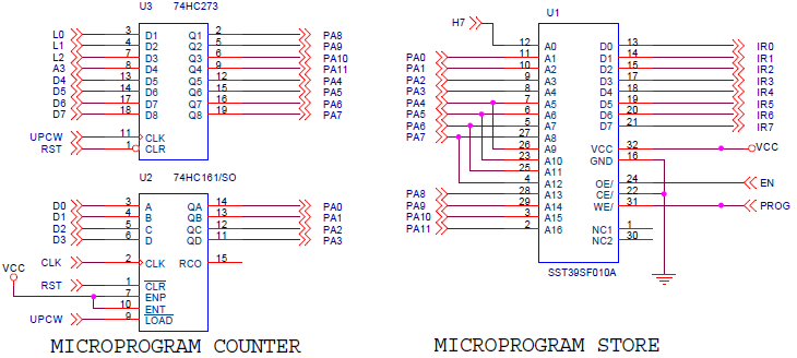
- Microprogrammed
UNUSUAL FEATURES
- Two rows of 20 pins each, with 0.05 Inch (1.27 mm) pin distance
- Microprogram is in FLASH memory and can be written with a Raspberry Pi as programmer
- Programmer's registers are in RAM
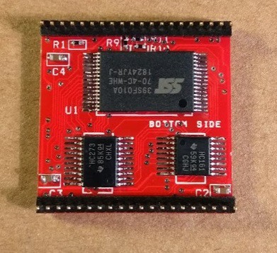
- There is NO ALU
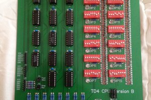
- Only 8 IC's, on both sides of a 1 square inch, 2-layer pcb.
The registers are in RAM. That has been done before (see TMS9900). This will not give you a speed devil, but it is needed to fit the design in one square inch. Another thing left out of the CPU for this reason is...... the ALU. ( I do not intend to connect the square-inch 4 bit TTL ALU to this cpu ).
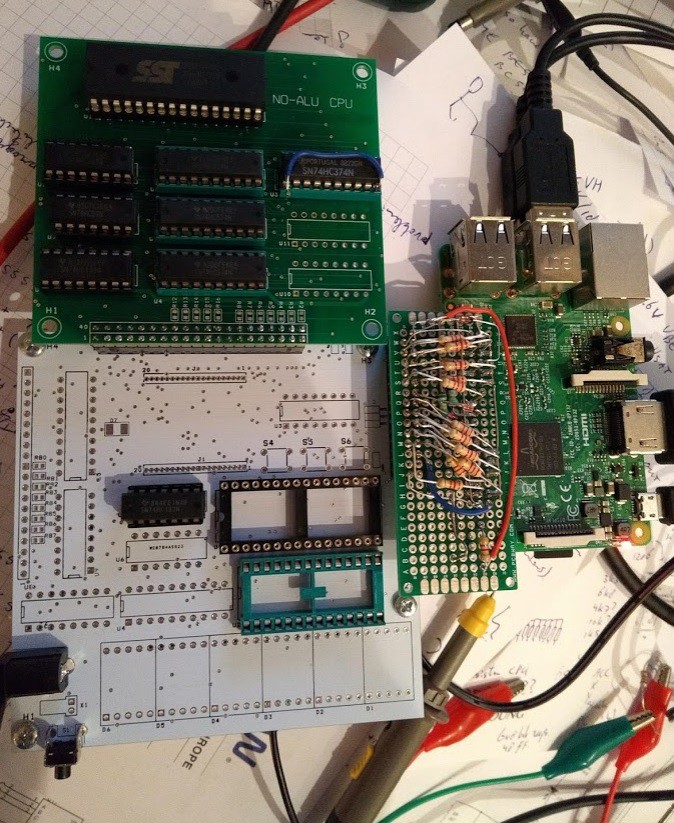
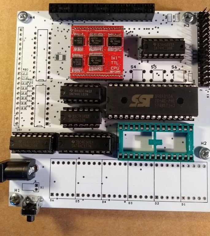
DEMONSTRATION PROJECT
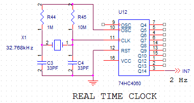
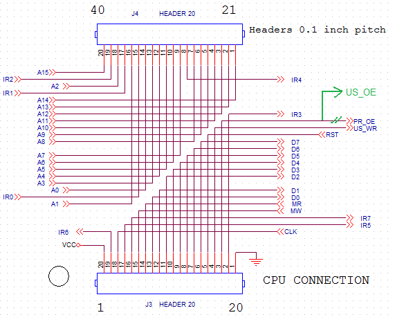
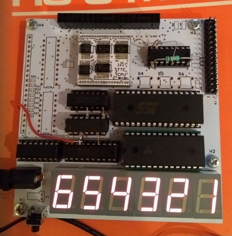
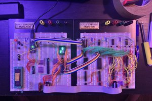
A development board was made, that has the external ROM and RAM for the CPU. It also has a 32kHz crystal with divider, and 6 displays, to make a digital clock. The clock is working now ! The development board also has an I/O connector, so it can also be used for other projects.
PROGRAMMING ENVIRONMENT
To make programming easy, an online Javascript editor/assembler/simulator was made. The assembly code for the application can be made and assembled in your browser. It can also simulate the cpu. If you open the simulator, just press Assemble and Run to see the simulated working clock (no soldering required) !
If you do this on a Raspberry Pi, you can save the assembly code to your local memory card, and you can download the assembled binary code. The Raspberry Pi can be connected to the development board, and directly burn the binary code into the flash ROM of the development board by means of a Python script.
While connected to the development board, the Raspberry Pi can also program new microcode into the square inch cpu. The required software and Python scripts are available in the files section.
THERE IS NO ALU
NO ALU... I could have programmed a small PIC or AVR as ALU (Wikipedia: ALU), but that's cheating. With the current microcode version, the only arithmetic that it can do is compare bytes and address items in a table. And the hardware won't allow much more.
For incrementing or decrementing a byte, lookup-tables are set up that contain an incremented or decremented version of the lower 8 address bits. Now the processor can increment or decrement a byte. Nothing more is needed to do arithmetic !
This was also done in the legendary HP9100 programmable calculator that was introduced in 1968. It worked with transistors and diodes, not a single digital IC ! The story behind this calculator is amazing, and can be read on hp9825.com. People have tried to reverse-engineer the diode-transistor logic and came to the conclusion that the hardware of the machine could only increment or decrement digits (described by Tony Duell). Yet it could calculate with...
Read more »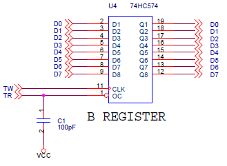


 Tim Ryan
 agp.cooper
I found another design https://www.bigmessowires.com/nibbler/
instead of using micro-program for executing an instruction, it just decode the instruction into a set of control signals, so the uROM or micro-code concept there is more like instruction decoder, the primary reason why nibbler can does that and 1square-inch can't is that:
Nibbler has very rich internal inter-connect, so a meaningful operation can be done in one clk cycle, but 1square-inch's internal structure is too simple to perform a meaningful instruction within one cycle, that's why micro-program is required, not just micro-code.
from which I realized that the basic nature of instruction is a set of control signals setup before next clock ring-edge so then the state of CPU will be updated accordingly. the whole CPU is a FSM, and instruction are the ways to change it's state.
Even more, sometime we don't need a full Tuning-complete CPU to solve a problem, in that case a simpler FSM can be designed w/o the BUS/RAM even ROM