spudfishScott
-
Register Memory Function Test
01/18/2019 at 22:08 • 0 commentsI'm almost completely finished with Register Memory. All there is left is to finish the final three-bit boards for four registers (you can see these as "wire only" breadboards on the far left). Meanwhile, here's a video of a quick test. I used an Arduino to make clock pulses and to put a random number at the Register Memory Input on each cycle. I used another Arduino to pick a random register to write to and two random registers to send to the Channel A and Channel B outputs. So far, so good!
-
Designing and Building Register Memory
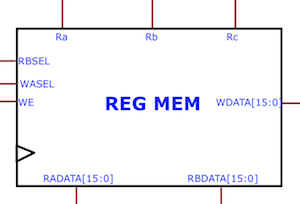
01/09/2019 at 16:17 • 0 commentsFrom a functional standpoint, the only differences between the Spikeputor's Register Memory and the Register Memory of the "Beta" processor on which it is based is a decreased number of registers (8 vs. 32) and a decreased number of bits per register (16 vs. 32). Otherwise, the inputs and outputs are the same. RegMem has three register address inputs (Ra, Rb, and Rc), three bits each, a 16 bit data input (WDATA), two 16 bit outputs (RADATA and RBDATA), three control lines (RBSEL, WASEL, and WE), and a clock input.
![]()
Functionally, register Ra is immediately placed on RADATA. The RBSEL signal determines whether Rb or Rc is placed on RBDATA. WASEL selects whether Rc or R6 (used as the exception pointer on IRQ) will be written to, if WE is high, on the next rising clock pulse.
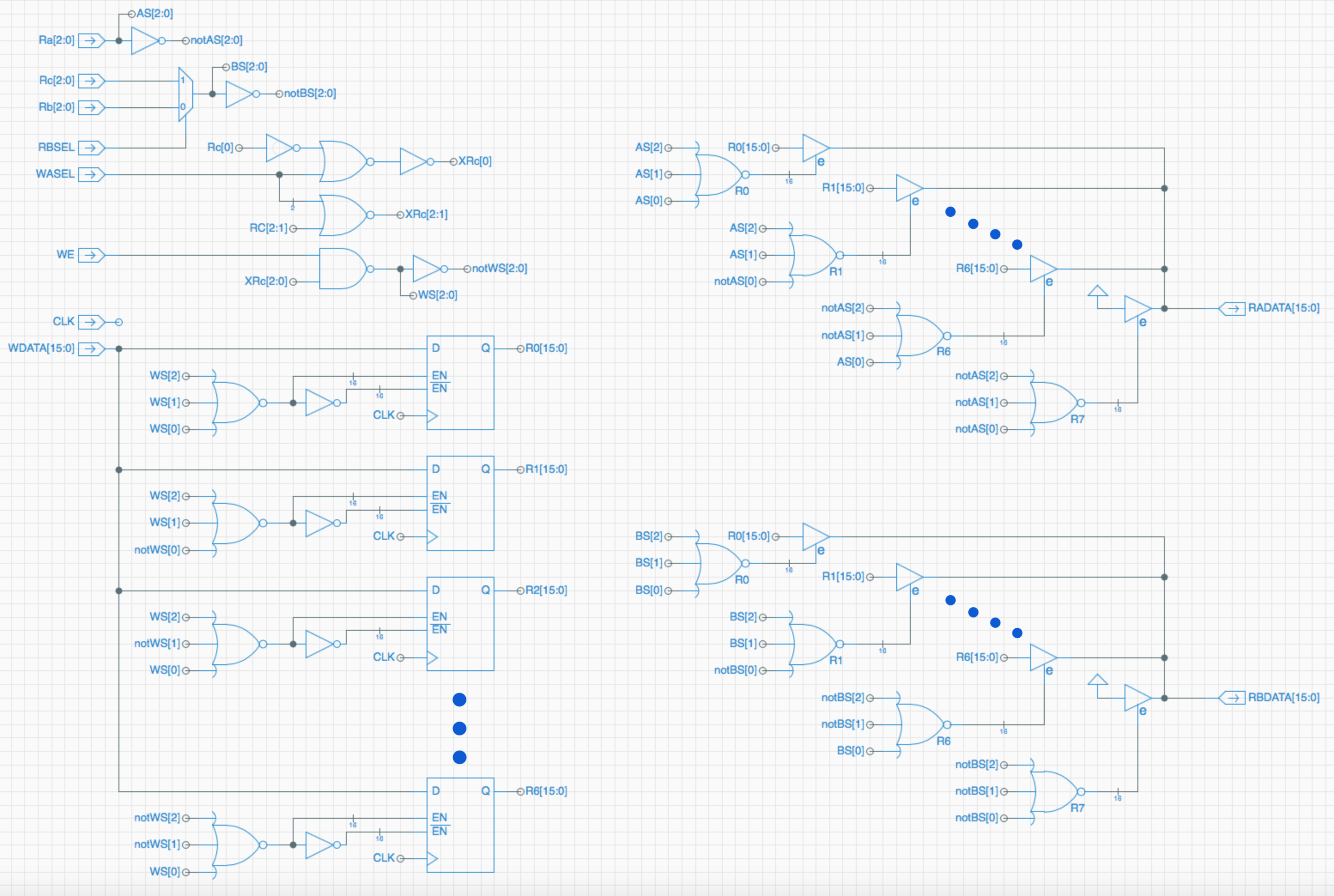
The full schematic of the register memory is shown below, and includes some logic to handle the control lines, decoder logic to translate each of the address signals into enable signals for the writeback and output functions, load enable positive edge-triggered flip-flops to store the data, and tri-state buffers to select each of the two output channels.
![]()
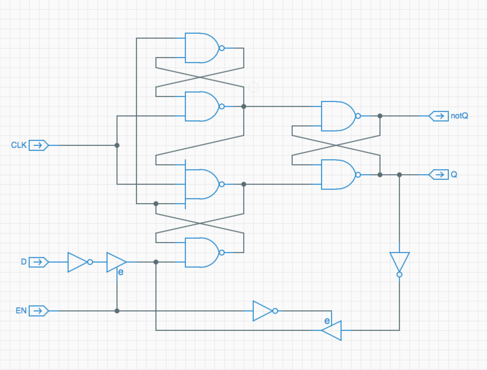
The flip-flops are modified from those described in the "Building Blocks" log entry to include a built-in MUX2, which selects between updating the flip-flop with new data (EN high) or previously stored data (EN low). Note that all of the tri-state buffers are implemented as a single transistor using source as the input, drain as output, and gate as enable. To overcome issues with the body diode in the 2N7000, each signal going into the tri-state must be a isolated from the rest of the circuit. This was done by simply putting an inverter in front of each tri-state input. Yann Guidon pointed out that I could have also used two transistors, rather than a transistor and an inverter. I had explored this earlier, but abandoned it for reasons I can't quite remember (might have had to do with a lower voltage output for that configuration). Since it spares a resistor, I'll likely use it for later additions to the Spikeputor CPU.
Since notQ is the actual desired value of the bit (because D is inverted before the tri-state), an LED was wired directly to that output to show the state of each bit. The two channel outputs actually come from Q, followed by an inverter leading to the tri-state buffers shown in the schematic. Note that for R7, the data values are hard-wired to ground, nor is there any circuitry for writing to or storing in R7, creating the "always zero" register.
![]()
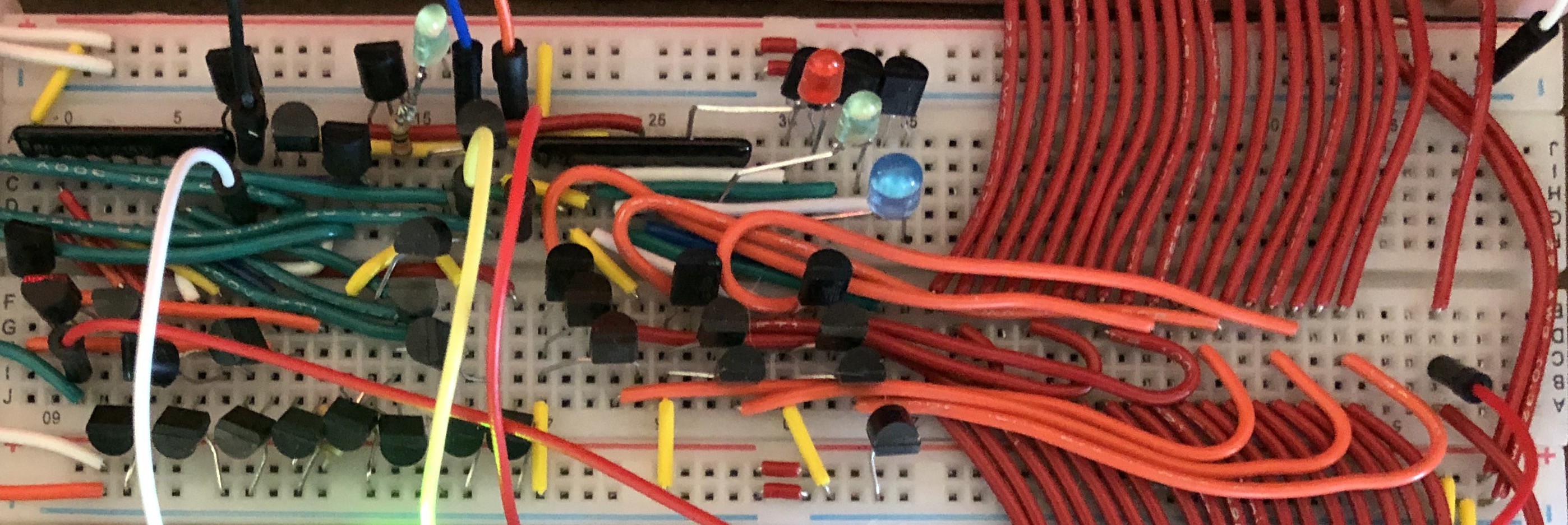
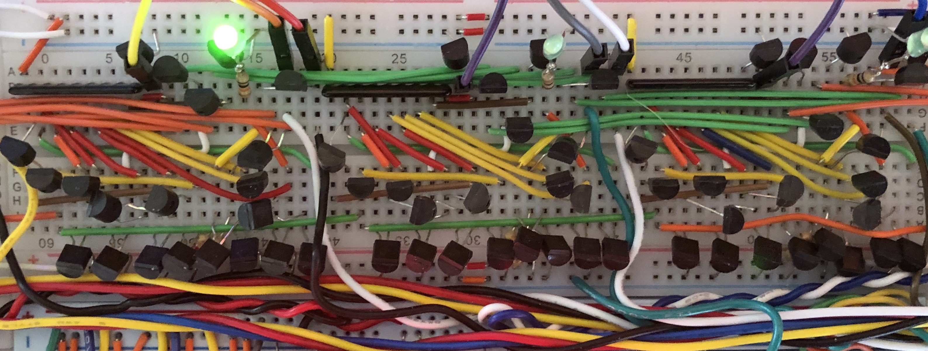
Each register is arranged in a single row on the pegboard, with one breadboard containing the decoder logic and bit 0 of the stored value, and five breadboards with three bits each completing the remaining 15 bits. The decoder also has three LEDs to indicate if the register is selected for writeback (blue), or channel A (red) or B (green) output.
Decoder logic and Bit 0:
![]()
Three bits of Register Memory:
![]()
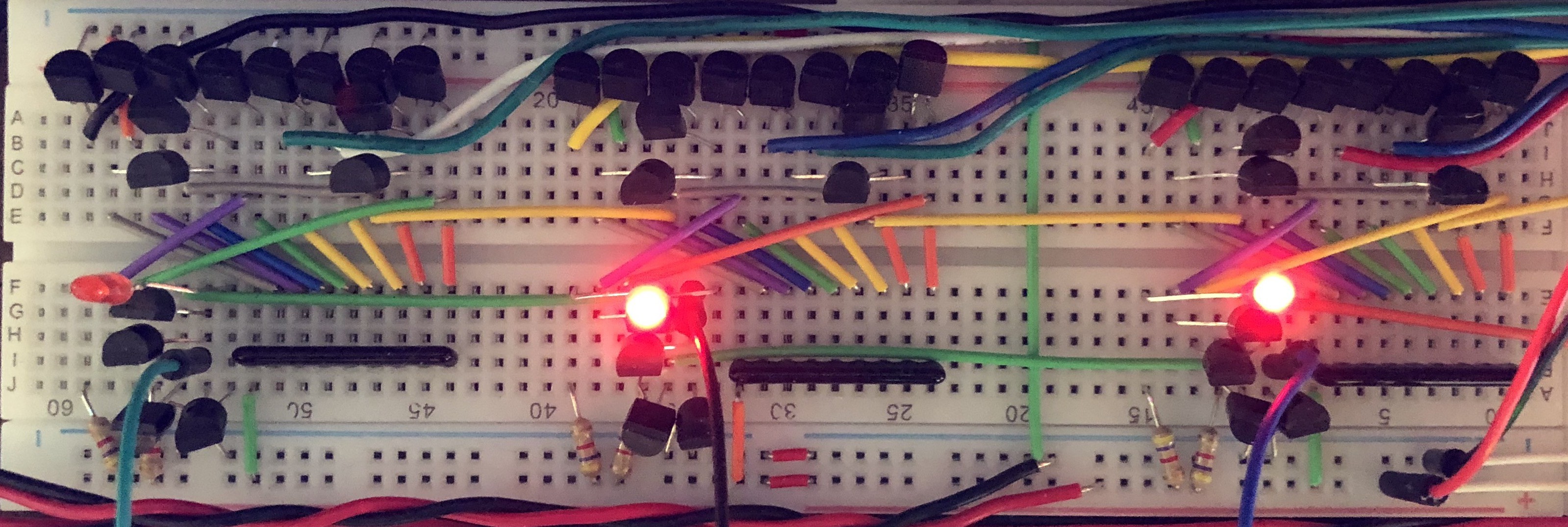
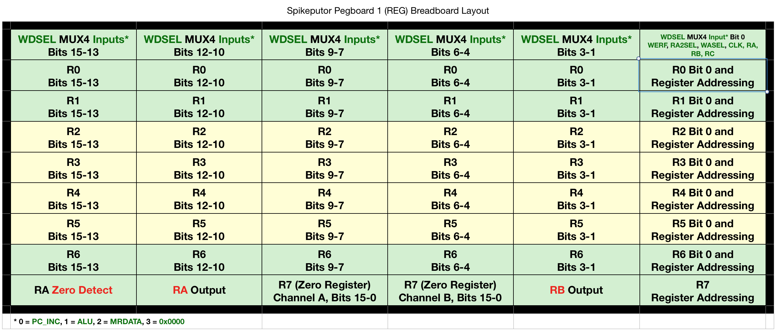
Because I had space, the Writeback Data MUX4 used to select the RegMem WDATA input was placed at the top of the RegMem pegboard. It is also five breadboards wide (three bits per board), plus an additional board for Bit 0 plus the rest of the logic to process the RegMem control signals. The WDSEL signal selects which input (PC_INC, ALU, or MEMORY) is used for WDATA. At the time of the initial design, the fourth input on the MUX4 was open. Since I had the space to accommodate it, I kept it open, initially grounding each bit of the signal, figuring I'd have another way to write a zero to a selected register. As it turns out, as of today, I think I'm going to need this open position to capture the current PC value to handle interrupts, but that's still being worked out. Bottom line: I'm glad I had the inkling to leave it rather than spare some transistors to build a MUX3 instead.
WDATA Input from WDSEL MUX4:
![]()
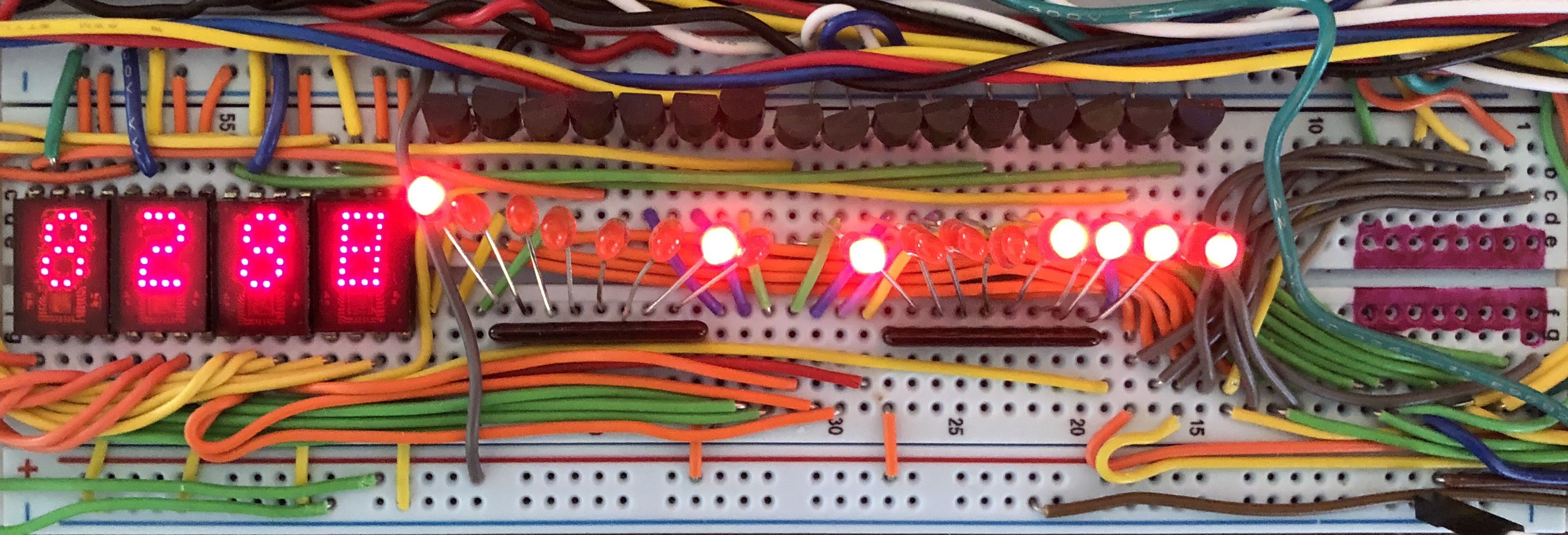
Since register R7 is zero only, it only needed two boards (one for each output channel) to lay out all of the associated tri-state buffers. That left room for two boards to display the RegMem output, both in binary using 16 LEDs, and as a hexadecimal number using HP-5082-7340 display chips (they were way too expensive, but I got them anyway because They. Are. So. Cool.) Note: that last digit appears all-on because when the photo was taken, the associated register was rapidly cycling through all 16 values of the least significant digit. Also note the red-colored area on the board which will serve as the output bus from this channel of RegMem.
![]()
Lastly, there was one more open space on the bottom of the pegboard to house the RADATA Zero Detect logic, which is just a big NOR tree:
![]()
Here's how things stand as of today. I have completed all 16 bits of registers R0, R1, and R6, four bits each for R2, R3, R4 and R5, and all of the input and output components, including "always zero" R7.
![]()
After completing the first two registers and the input and output rows, I started working on the ALU, which will be the subject of the next few logs. As I post those, I'll also be working on finishing the Register Memory. Then, it'll be time to build the control logic that will turn this monstrosity into an actual CPU!
-
Overall Design and Build Strategy
01/08/2019 at 03:36 • 0 commentsAs mentioned in the Details Section, the Spikeputor CPU is modeled after the "Beta" CPU from the MITx course, "Computation Structures" (see this link to the Beta diagram). The Beta is a 32-bit RISC CPU with 32 registers (31 + 1 that is hard-coded to zero). I chose it as a model because, frankly, it was the only CPU I knew from the ground up and it seemed relatively simple and elegant, yet quite powerful. Once I did a quick calculation of the number of discrete components I'd need to fully implement the Beta, however, I knew that some compromises would have to be made. The main compromise was to switch from a 32-bit to a 16-bit architecture. At that point, I did NOT look at other 16-bit CPU designs. Instead, I took on the challenge of adapting the Beta to a 16-bit design with as few changes as possible. The biggest changes centered around opcode and instruction size. The beta always executed one opcode per clock cycle. The 32-bit opcodes were wide enough to accommodate instructions featuring up to three registers (five bits to address each of the 32 register locations) or two registers and a 16-bit constant. The remainder of the bits were more than enough to describe all of the instructions defined by the Beta's ISA (Instruction Set Architecture).
With only 16 bits to work with in a Spikeputor CPU opcode, the number of registers needed to be reduced to eight (three bits to address each of them, R0 to R7, where R7 was hard-coded to always be zero), leaving six bits for encoding the rest of the operations. Obviously, there was no available space for constants of any size within the opcode itself. Reducing the register count was acceptable to me. There'd be a code efficiency hit, but the transistor count for Register Memory was much more manageable. To be able to use constants, however, required a major change in the architecture. Instead of a simple one instruction per cycle design, a multi-phase instruction scheme was needed, necessitating several additional special-purpose registers, independent from the user registers. I envisioned three CPU phases. Phase information would be stored in a two bit CPU_PHASE register. In phase 0, the instruction would be read in to a 16 bit INSTRUCTION register. If the instruction called for a constant, the CPU phase would be updated to phase 1, the program counter incremented, and the constant read in to a 16 bit CONSTANT register. If a constant wasn't part of the instruction, the CPU phase would go directly from phase 0 to phase 2. In phase 2, the instruction would be executed, including updating the Program Counter to go to the next instruction or to branch to a new memory location.
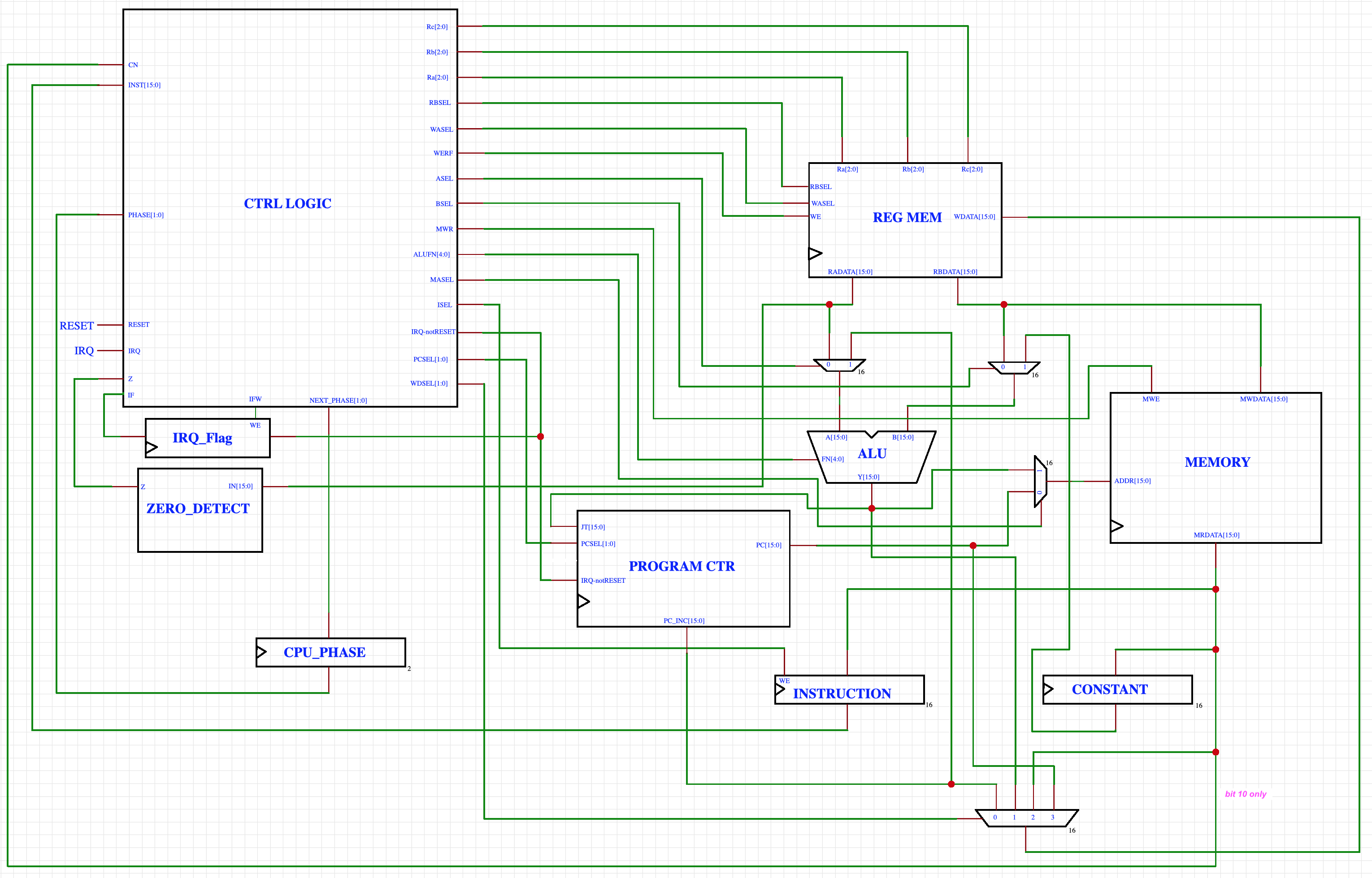
One other difference I chose with the Spikeputor CPU was to not implement a "supervisor" address bit, mainly because I wanted the flexibility to (eventually) use the entire 16-bit address space. Instead, to handle interrupts (which I still don't know if I'll even use, but still wanted to design), there would be a one bit IRQ_FLAG register to prevent the interrupt itself from being interrupted. The whole initial design looked like this:
![]()
I'll describe each of the modules in greater detail in subsequent project logs.
Since the Register Memory and ALU were most similar to the Beta design (something I gained experience with taking the Computation Structures course), I decided to dive right in to starting to build those first. As mentioned in the Details, I'm doing the whole project with solderless breadboards. I'm doing this for purely artistic reasons: I just love how they look, the air of impermanence they invoke, and their modularity. In addition to the schematic, I needed to plan out how the actual components would be laid out. Trying to use breadboard space most efficiently is actually another major design driver. Usually this goes hand-in-hand with transistor component efficiency, but not always. Sometimes, adding a few extra components actually makes it easier to lay out the boards without having to bend transistor leads in crazy ways. And leaving extra "white space" on a breadboard has been quite helpful in lining all of the components up, and also allowing for last-minute additions when required.
I had some 4’x2’ pegboards that I decided to use to mount the breadboards. They were big enough to hold 54 breadboards in a 6 x 9 array, plus some extra space for power supplies, and a few smaller breadboards if needed. I created a pegboard template to lay everything out. Here's an example for the Register Memory, which fits perfectly onto one pegboard. Green text is an input, red text an output. Green background means I've completed the actual boards, yellow means they're designed, but not completed yet, white (not pictured here) means not yet designed. As of today, most of Pegboard 3 and all of 4 is white.
![]()
The entire Spikeputor will take up four pegboards:
- Pegboard 1: Register Memory
- Pegboard 2: ALU
- Pegboard 3: Program Counter, Special-Purpose Registers, Control Logic, and Chip Memory
- Pegboard 4: "Screen" Memory
The four pegboards will fit neatly on a single wall in my house, with space below for a desk, which will hold the Apple II plus that I'll be using for I/O.
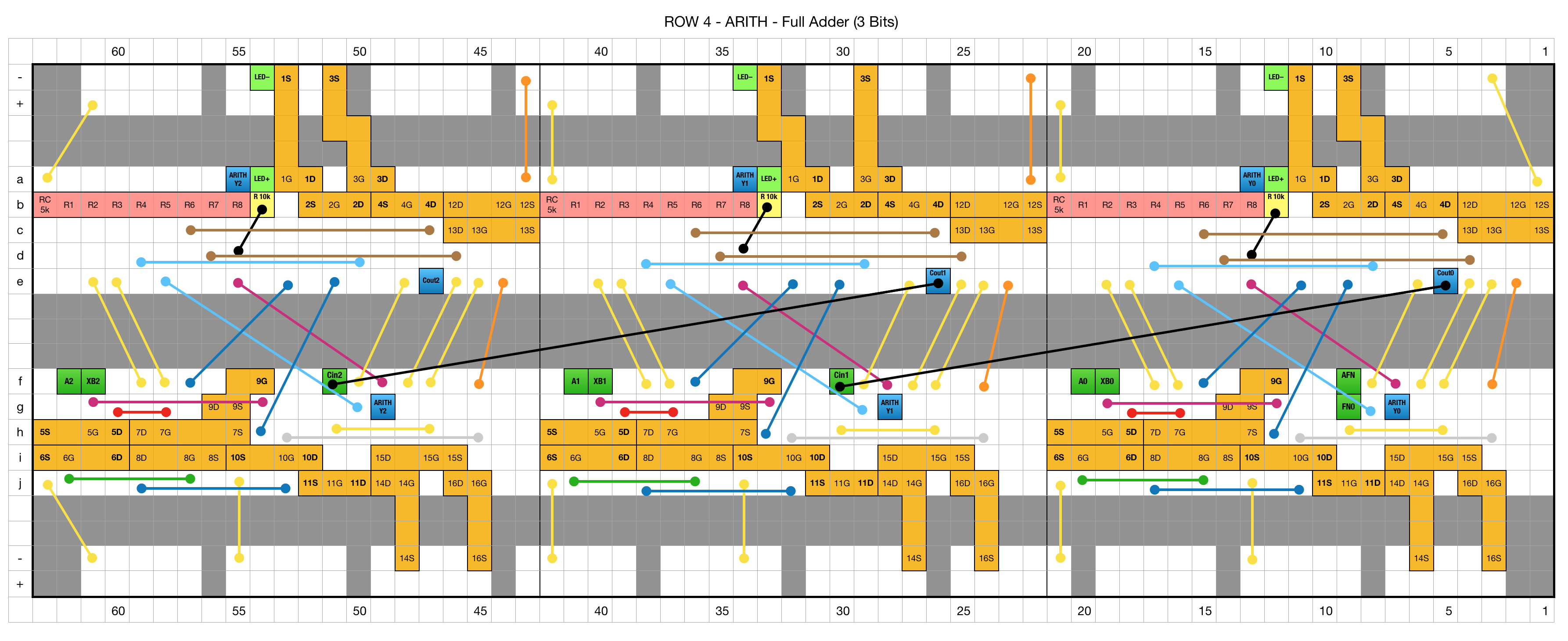
Finally, I have another template for laying out components on the breadboards. Translating schematics into breadboard layouts is a Tetris-like challenge that can be maddening, but ultimately quite satisfying! Here's an example of three bits of the ripple-carry full-adder circuit of the ALU. Orange = transistors, Red = SIP-8 resistors, Other colored boxes are either LED leads, discrete resistors, or inputs and outputs:
![]()
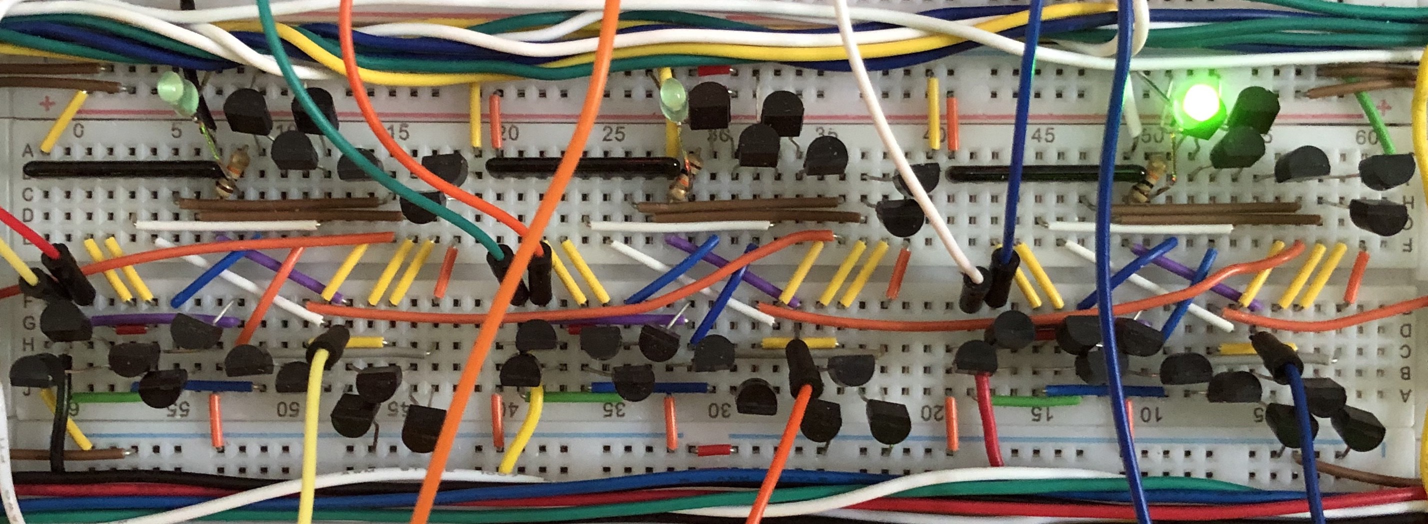
And here's the finished product:
![]()
OK. Happy to entertain questions and comments. Next we'll get to actually building the thing!
-
Building Blocks 2: Multiplexors and Flip-Flops
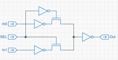
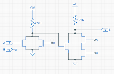
12/28/2018 at 16:35 • 10 commentsFrom simple transistor-based logic gates, we turn our attention to the higher complexity components that make up the essential building blocks of the CPU: multiplexors, to set up the appropriate logic pathway for each instruction, and flip-flops, which become the basis of all of the registers. For this project, the overarching design principal for designing these components is transistor efficiency: We need robust, reliable components made with the fewest transistors. Since, with a 16-bit CPU architecture, each component is effectively copied 16 times for each implementation, even a design with one fewer transistor can make a big difference in the total number of transistors. It also provides increased flexibility for laying out the actual components on the breadboards. After a fair amount of research and building test circuits, the two-input multiplexor circuit shown below was chosen. Instead of the "classic" design with three NAND gates and an inverter (seven transistors), it uses single MOSFETs as a poor-man's tri-state buffer. This works quite well as long as the input signals are buffered, inverting them on input and once again on output, for a total of six transistors. This design can be easily extended to a four-input multiplexor (15 transistors vs. 17 using NAND gates).
![]()
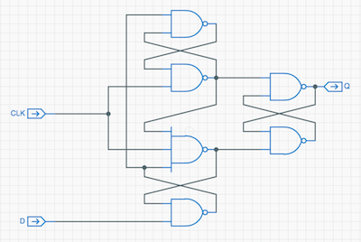
For the flip-flops, Wikipedia (borrowing from the TI 7474 chip) provided a nice transistor-sparing design for a positive-edge triggered D Flip-Flop for all the registers:
![]()
I was also able to use an XOR gate design that required only five transistors, which considerably simplified the layout (and transistor count) of the ALU's adder function:
![]()
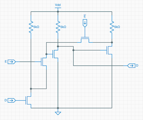
Finally, here's a five transistor design for one bit of static RAM that will be used for general purpose output, bank selection, and "screen memory" storage:
![]()
Armed with these basic components, it was time to start figuring out how it would all go together to make the Spikeputor CPU.
-
Building Blocks 1: Simple Logic
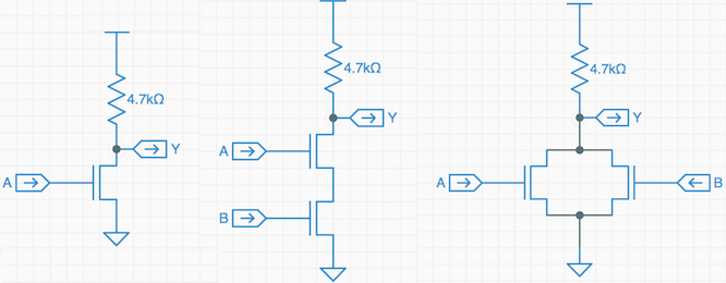
12/25/2018 at 20:00 • 2 commentsWhen creating a CPU out of transistors, the first thing one needs to do is pick a design for basic logic gates. I chose NMOS logic with 2N7000 MOSFETs. MOSFETs are nice because they don't require any current limiting resistors at the gate, since current flow from gate to source is basically zero. This reduces the total number of components and simplifies the design. The schematics for an inverter, a NAND gate, and a NOR gate are shown below:
![]()
The resistor value was chosen to keep the total power consumption of the Spikeputor in the light bulb range (25 Watts). Each logic gate in the CPU can consume V^2/R watts when all inputs are ON. That's about 5 mW per gate, and the Spikeputor will have on the order of 5,000 gates. Lower resistor values would speed up the gate switching time, but at the expense of greater power use. Based on modeling and measurements on actual circuits, I estimate that the maximum clock speed of the Spikeputor will be on the order of tens of thousands of hertz. Since the point of the Spikeputor project is to visualize computation, that's more than enough. Plus, getting up into hundreds of thousands of hertz clock speeds would require an order of magnitude decrease in resistance, bringing the Spikeputor total power consumption into the hair dryer range (250 Watts). Although all of these values are order of magnitude estimates, and we'll see the actual power consumption and speed as the thing gets built, I feel comfortable with these design choices.
-
Starting on Hackaday.IO: Current State
12/18/2018 at 17:12 • 0 commentsSince I started this hackaday project in medias res, as it were, I think I'll start with the current status and work both backwards and forwards. As of today, the register memory is about halfway complete (input, output, and three of seven registers, plus a zero register), and the ALU is 80% complete (just a few more shifters to install). Here's a video of the first Spikeputor "program", which is really just a hard-wired loop between the register memory and the ALU. Nonetheless, I have something that can perform successive additions on each clock cycle.
The Spikeputor
I am building a computer featuring a 16-bit RISC CPU made of discrete transistors for learning, fun and art. It will be pretty large.