 spudfishScott
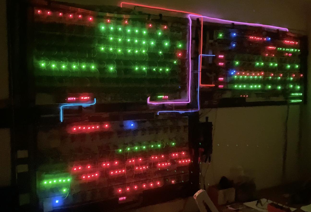
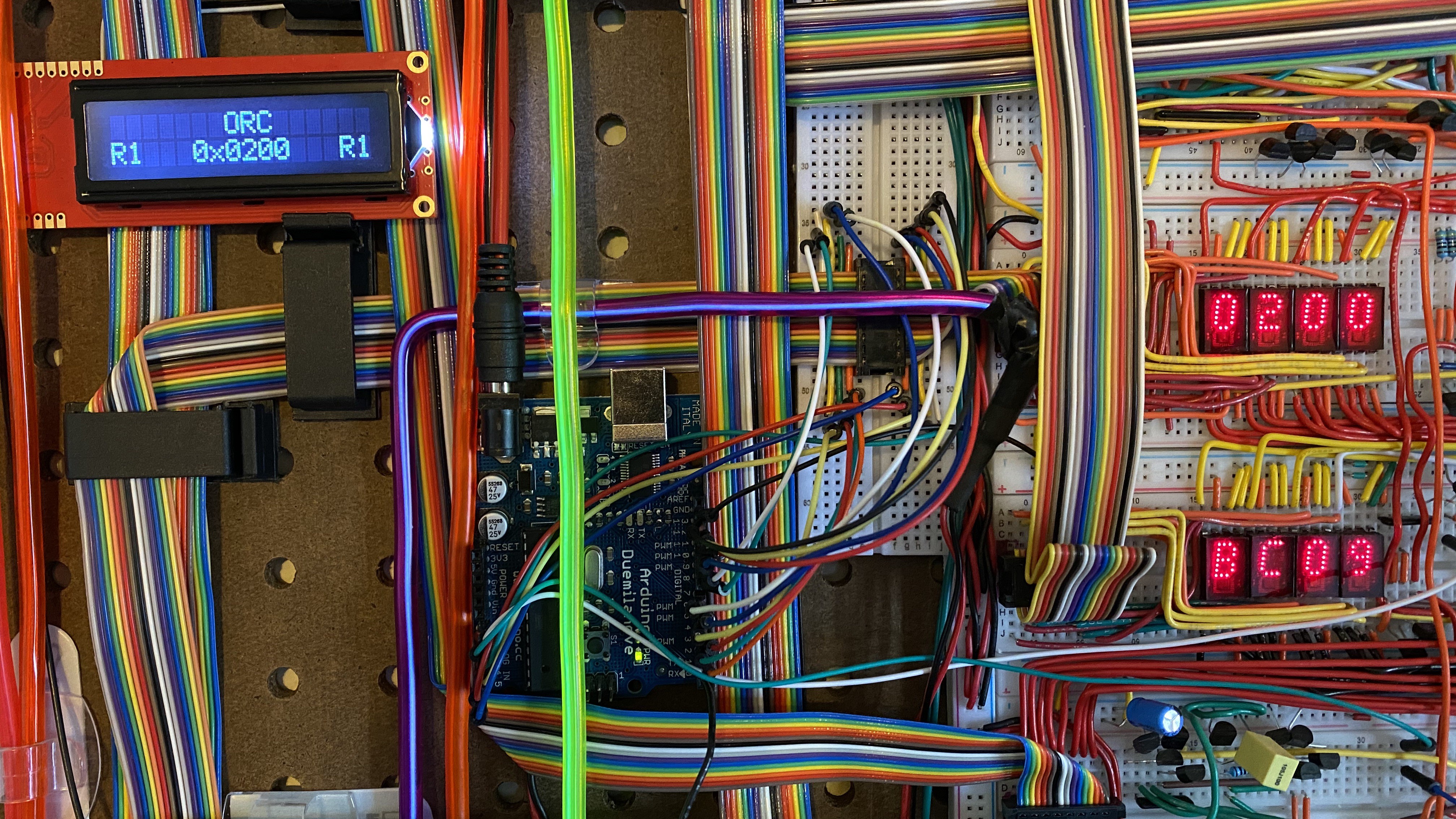
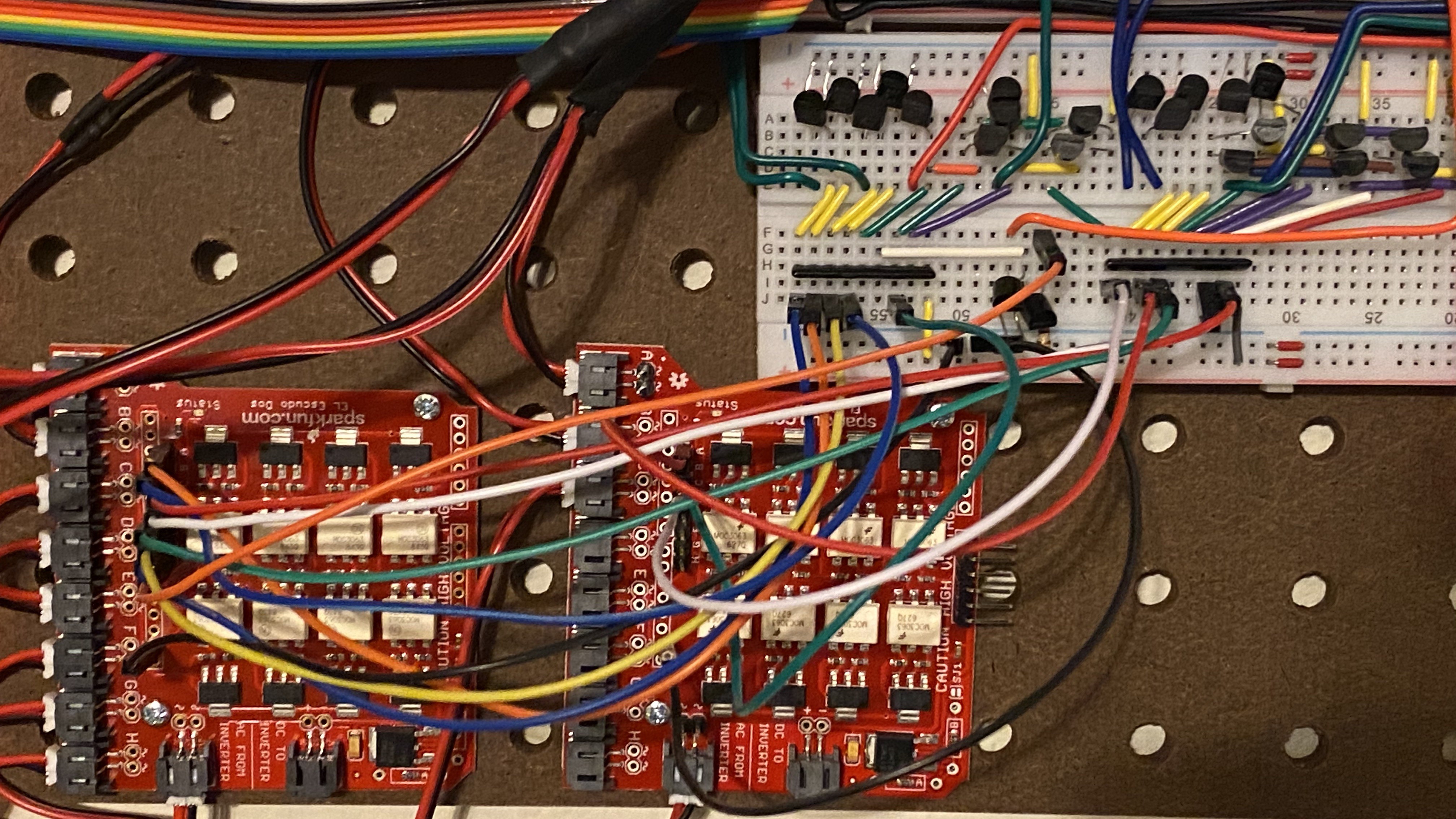
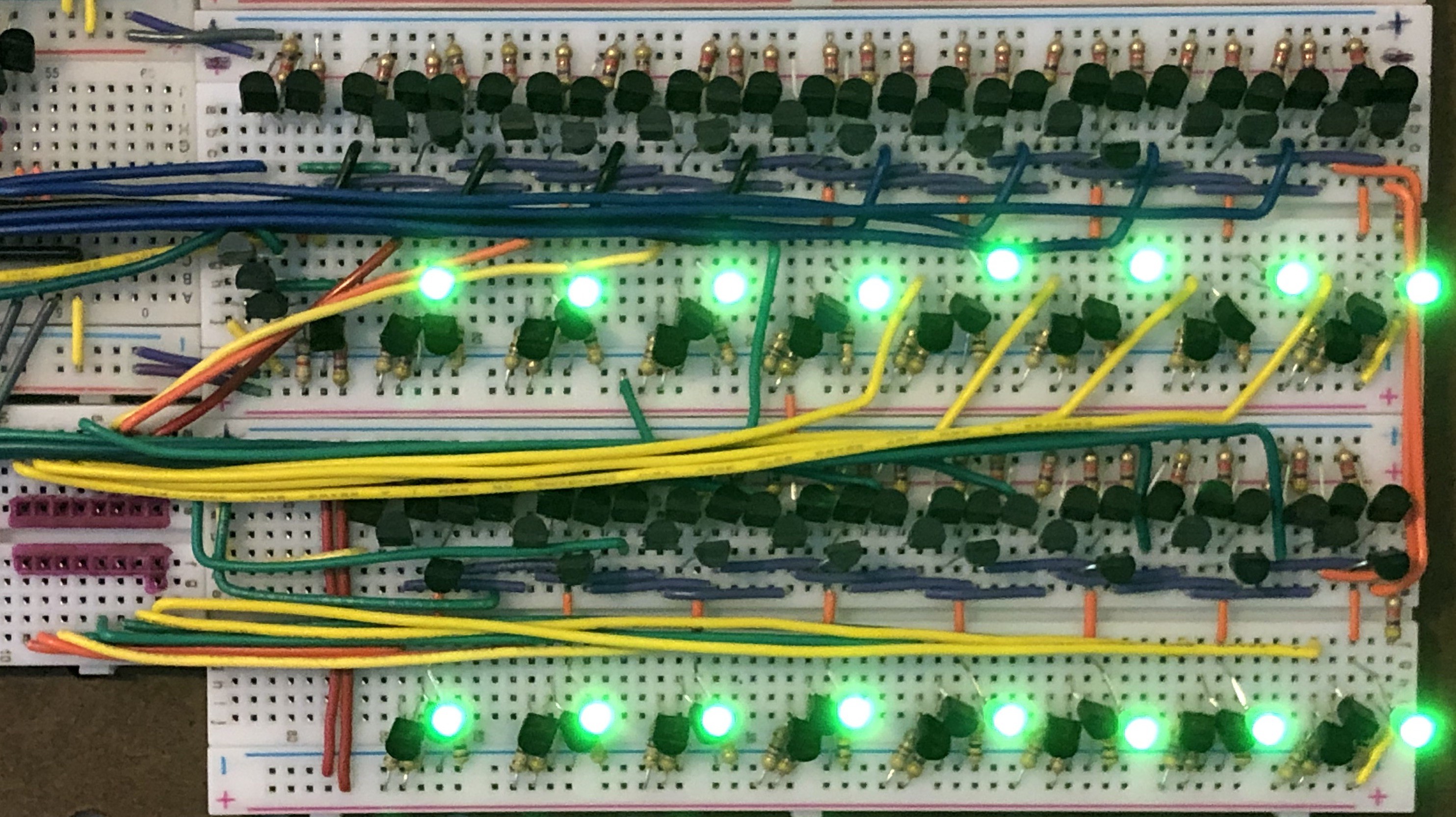
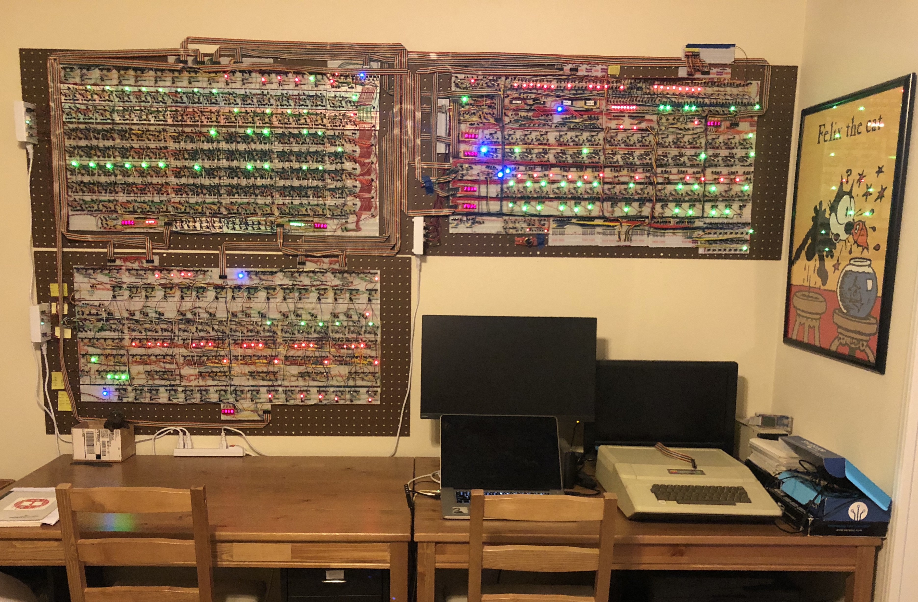
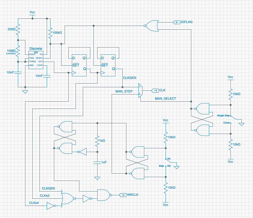
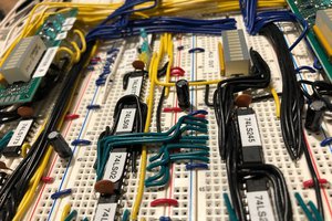
The Spikeputor will be a fully functional computer with a CPU made exclusively from NMOS logic using about 5,000 MOSFETs (2N7000), resistors, and LEDs to visualize the logic. HP-5082-7340 Hex Display chips will be strategically added to display the numeric contents of the outputs of the major CPU components, although if you read binary, the LEDs will provide the same information. Electroluminescent wire will be added to visualize the logic pathways between the major components. The clock will be adjustable from maximum speed (predicted to be in the tens of thousands of hertz range) down to single step. Since the primary driver of the Spikeputor is to visualize computation, speed was not a concern, although some steps will be taken (a clock tree, e.g.) to enhance the overall performance.
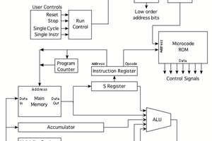
The initial CPU design was inspired by the Beta CPU, introduced in the MITx course, "Computation Structures" (highly recommended!) The Beta has a load-store, 32-bit RISC architecture. To save space, transistors, and the creator's sanity, the Spikeputor CPU was reduced to 16 bits. This necessitated several other major design changes, mainly centering on the fact that 16-bit opcodes could no longer support the inclusion of constants within the opcode.
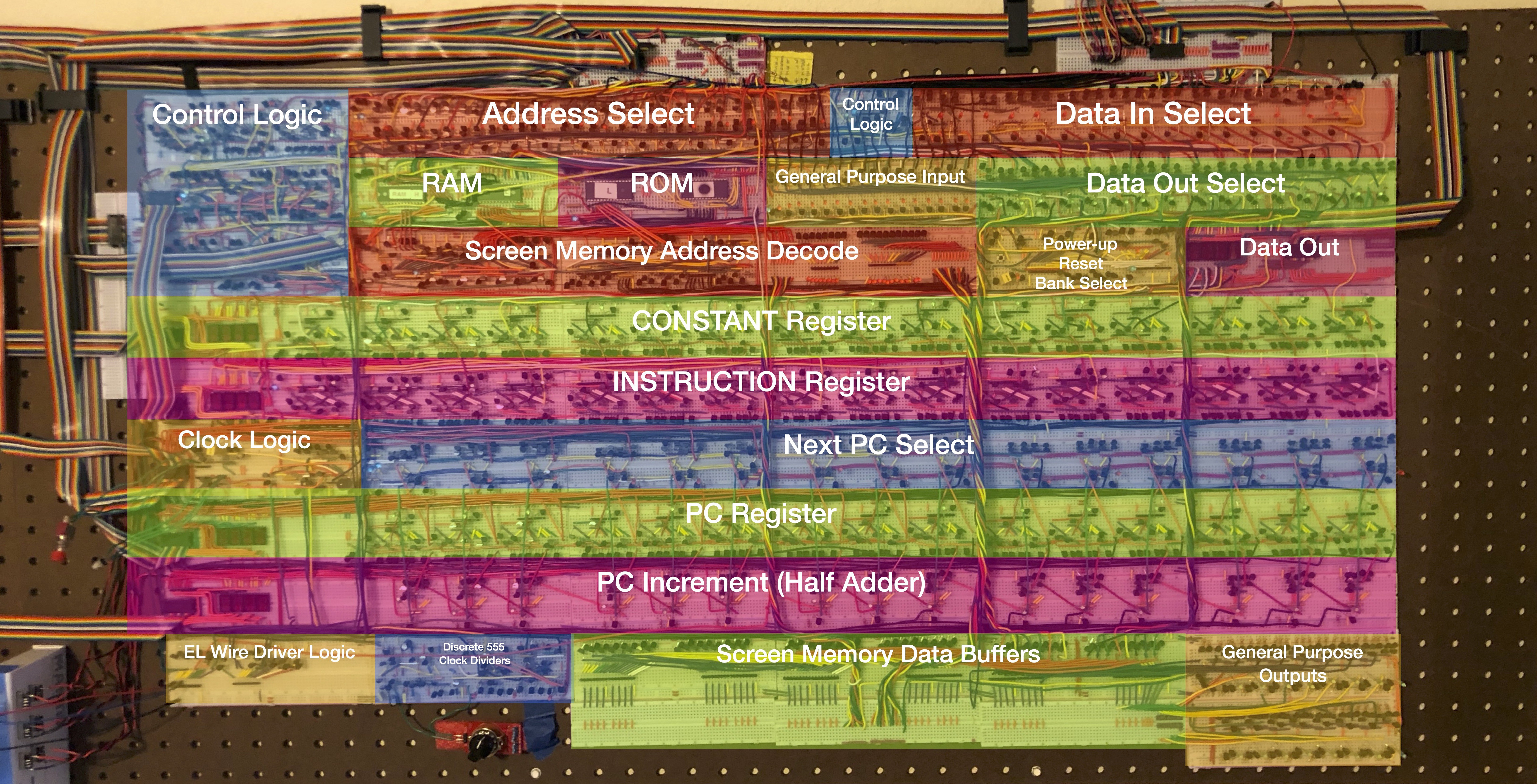
Spikeputor CPU Design Features and Major Components:
- 16-Bit Address space
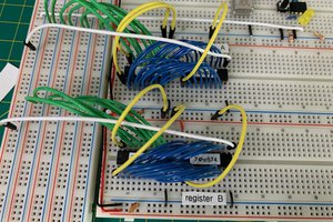
- Register Memory: Seven 16-bit registers, plus one register hard-coded to zero.
- Multi-function ALU
- Addition and Subtraction, supporting 2s Complement negative numbers
- Comparison (Equal, Less Than, Less Than or Equal)
- Boolean Logic (AND, OR, XOR, Identity)
- Variable Bitwise Shift Right or Left with or without Sign Bit Propagation
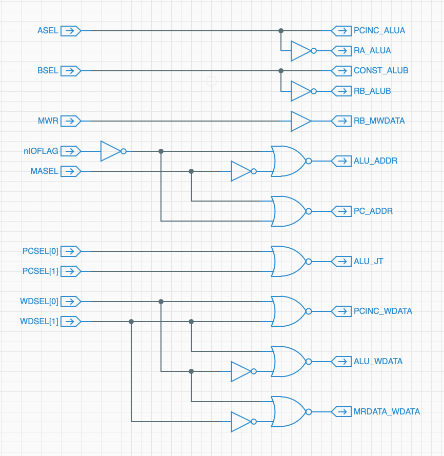
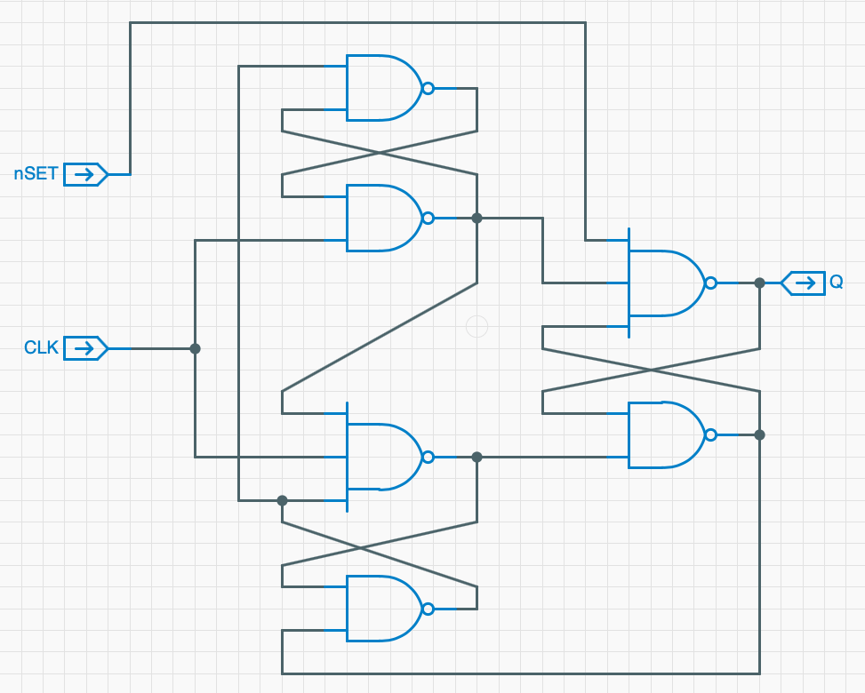
- Control Logic implemented with simple logic gates (no microcode or ROMs)
- Additional registers for Program Counter, Instruction, Constant, CPU Phase, and a few required status flags
- One-word opcodes for operations between registers
- Two-Word opcodes for operations between registers and 16-bit constants
- ALU Functions (see above)
- Memory functions: Load, Load Relative to PC, and Store
- Conditional (BEQ, BNE) and non-conditional branching with branch point storage
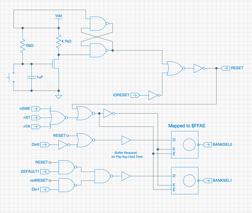
- IRQ and RESET handling (including automatically using register R6 as the Exception Pointer)
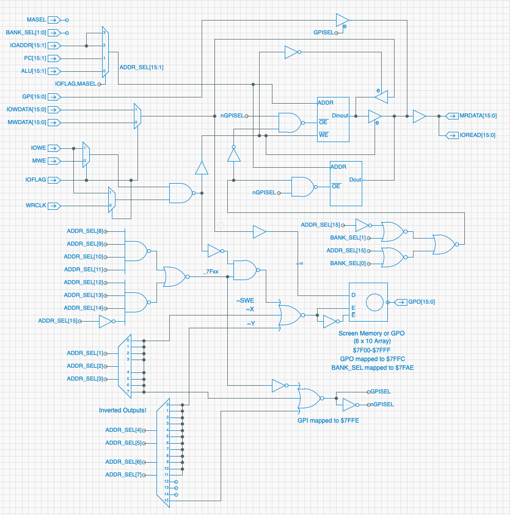
- Direct Memory Access (DMA) for all I/O
Memory
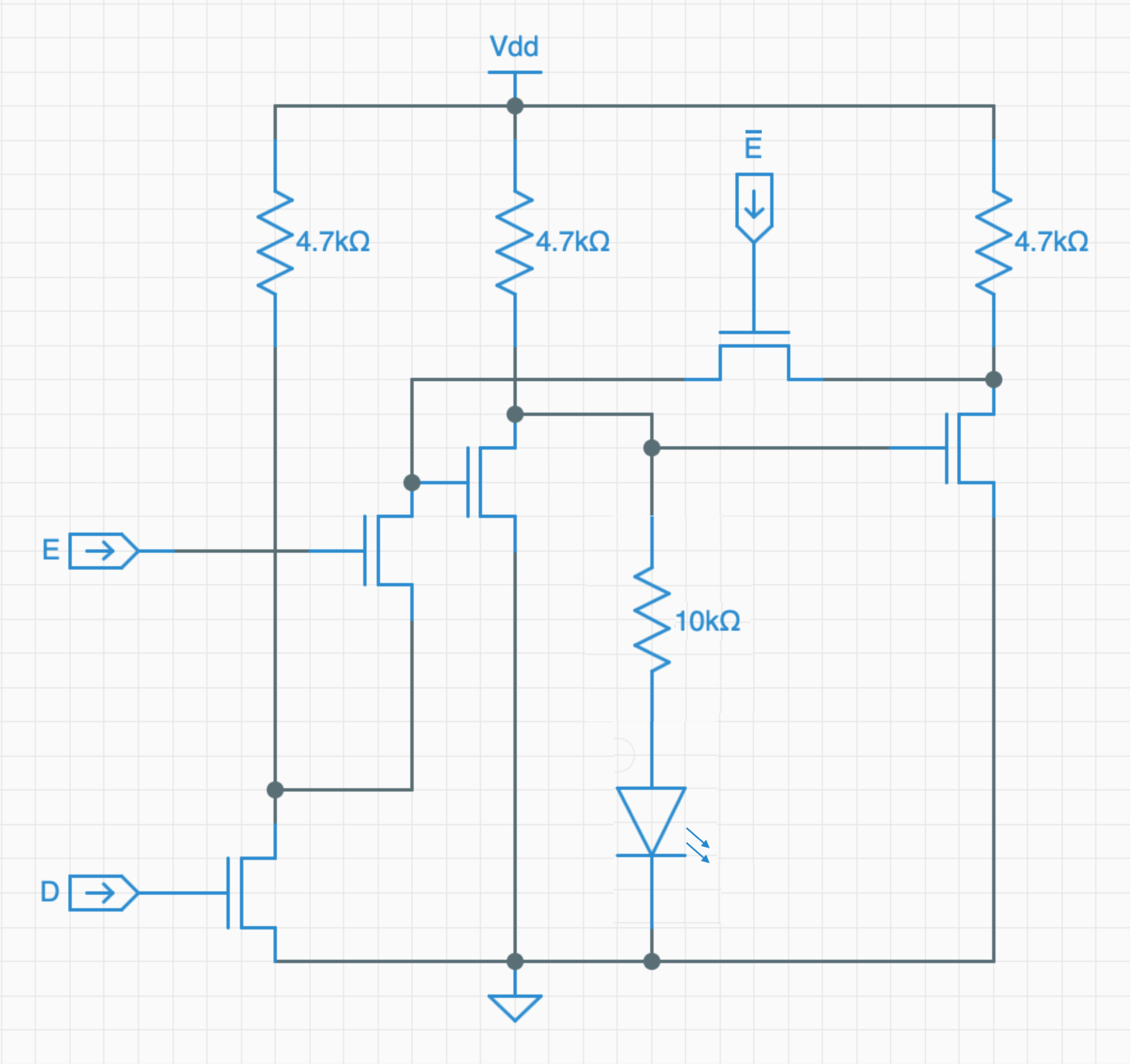
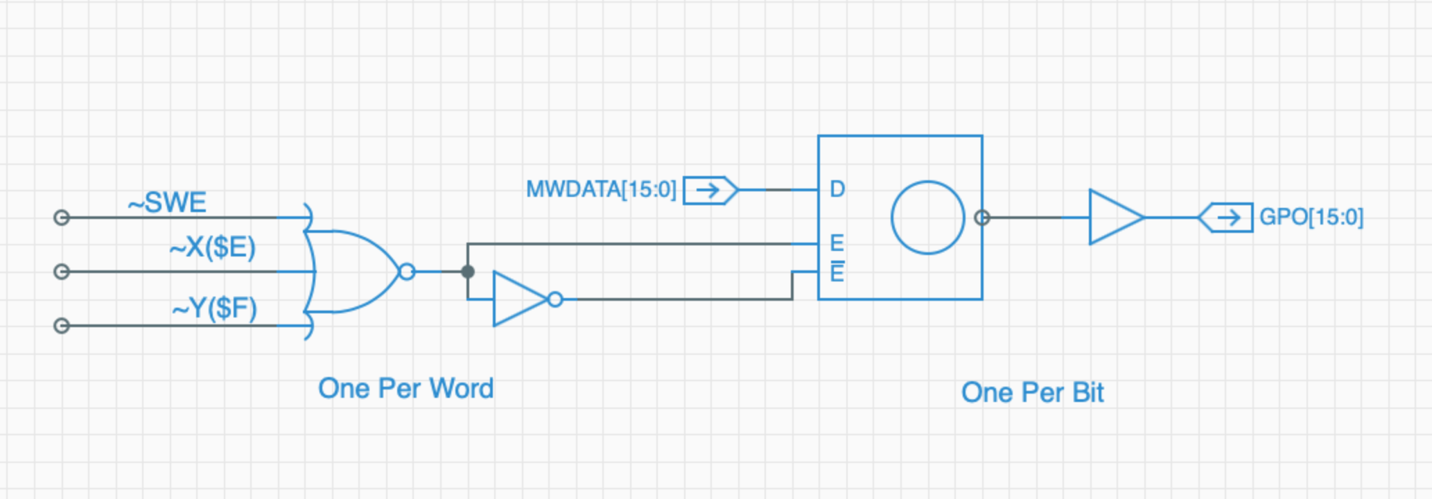
To be able to execute more than just trivial programs, the Spikeputor CPU will interface with high speed static memory RAM (2 x 32K AS6C62256) and ROM (2 x 32K AT27C256R) chips. In addition, a mirrored write-only "screen memory," also made from (roughly 5,000) transistors, will be created, providing a 48 by 18 array of addressable LEDs. Memory addresses will be restricted to word-boundaries. Attempts to address odd-numbered memory locations return the corresponding even-numbered 16 bit word. Since there weren't any 16K SRAM and ROM chips available, I used 32K chips, and will design a memory banking system to select 16K banks from the RAM and ROM for read operations. The full 32K words (64 kbytes) of RAM can be written to at any time.
Input/Ouput
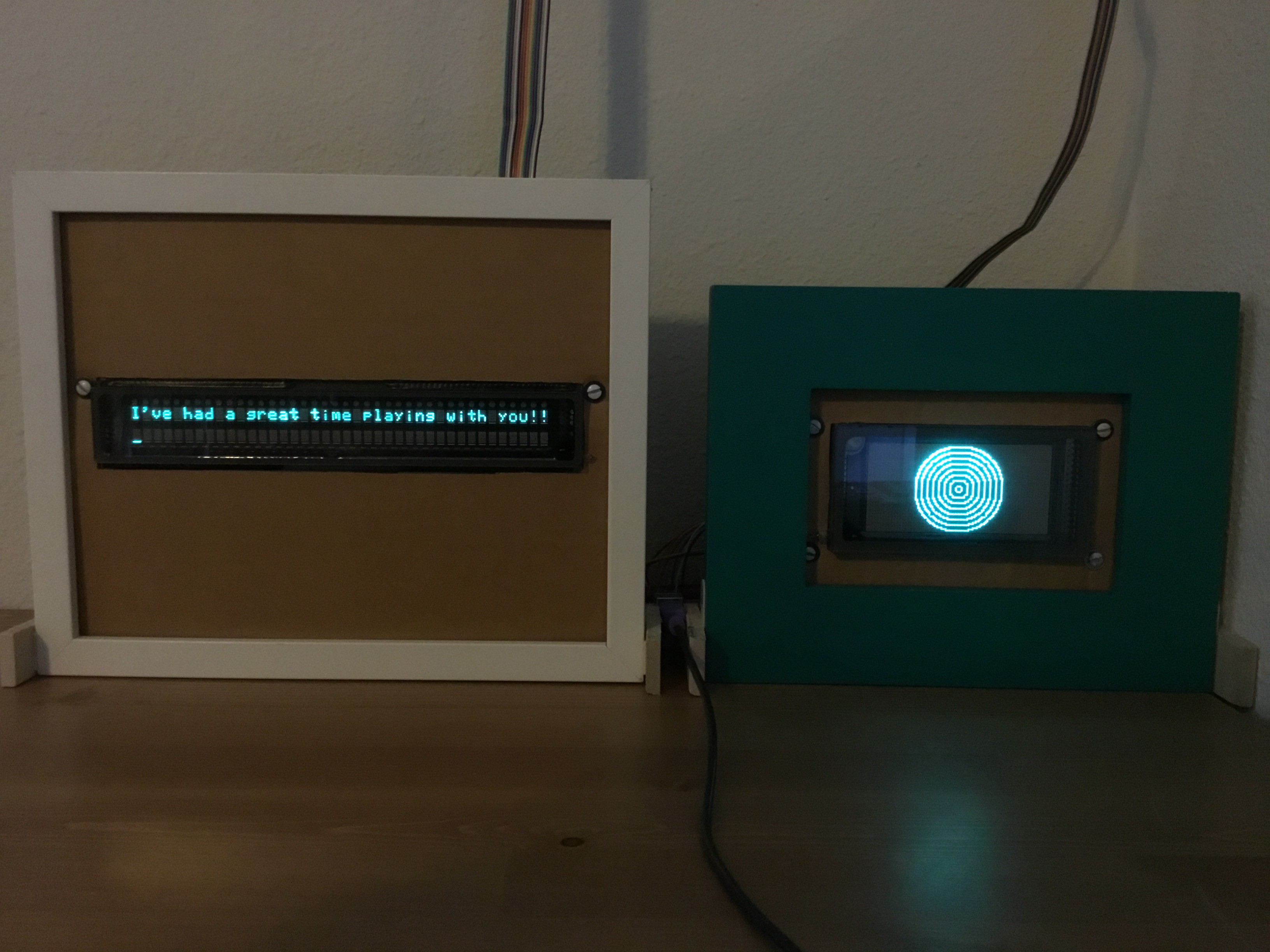
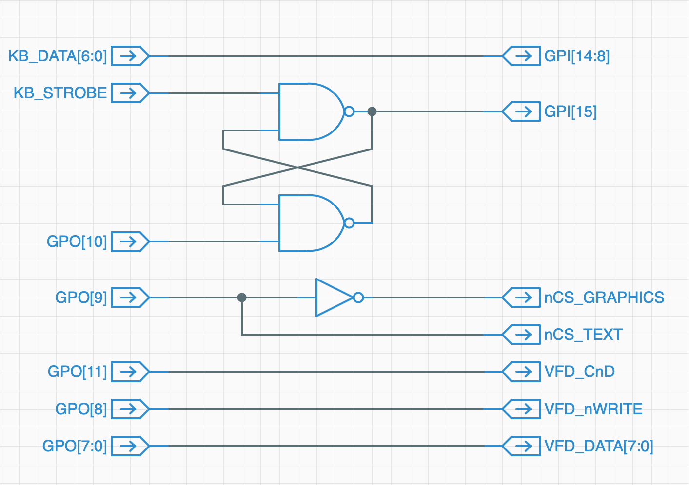
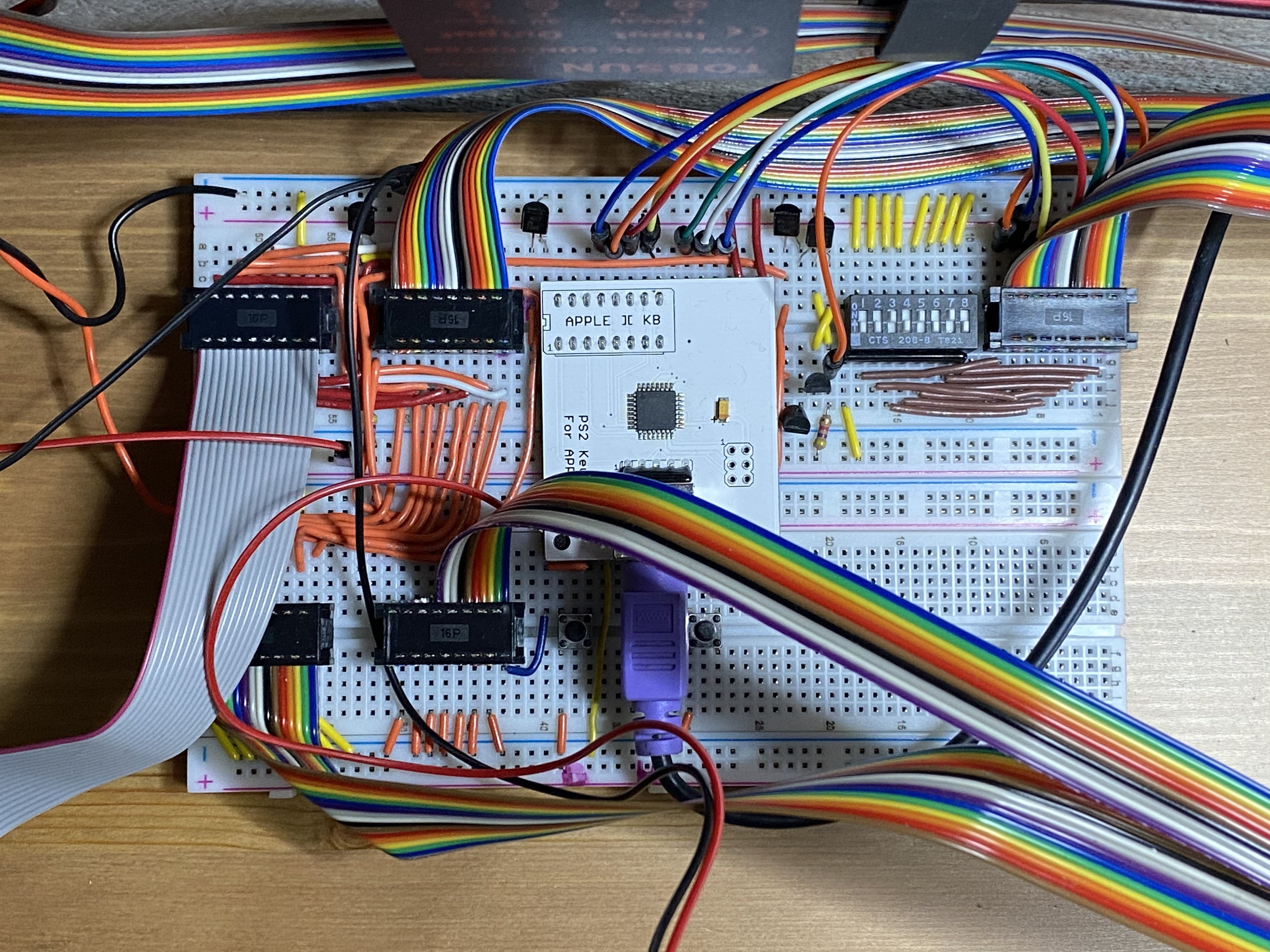
I/O functions will be facilitated via custom software and hardware running on an Apple II Plus computer, vintage 1986. A custom peripheral card called BIAS (Board to Interface Apple to Spikeputor) will be designed as part of the project, as well as the software on the Apple to provide keyboard input, screen output, and long-term data storage and retrieval. The I/O controller will have direct access to the Spikeputor memory and will halt the Spikeputor CPU during all read and write operations.
16 Bits of General Purpose Input and Output signals will also be implemented, mirrored to fixed high memory locations.
Structure
The Spikeputor will be assembled on a series of mounted solderless breadboards. Each major component (ALU, Register Memory, Control Logic/Program Counter/Status Registers, and Screen Memory) will be laid out on a 4 foot by 2 foot pegboard. Each pegboard can contain...
Read more »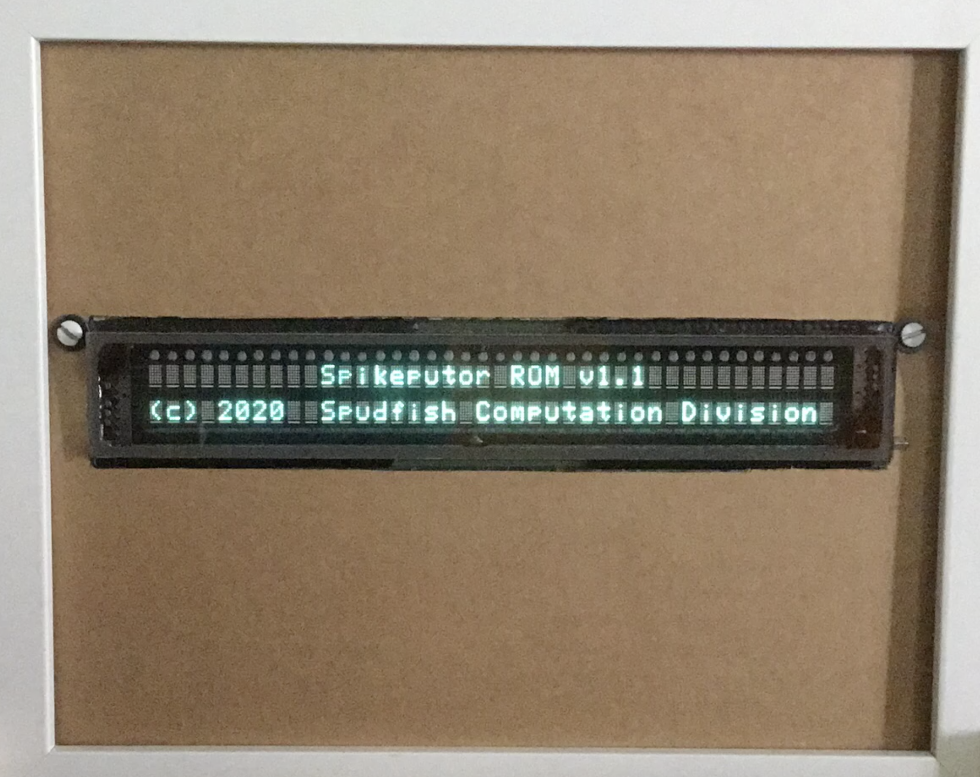


 Ced
Ced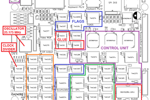
 Brandon Reinhart
Super cool project. I like how the electroluminescent wires make your computer look like an animated block diagram while it runs. Do you have a guess for how many transistors you used (assuming math has discovered numbers that large)?