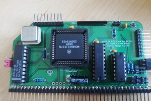
The basic design of the board is much the same as the 65C02 board combined with the standard glue used to attach 65C816 processors to a 6502. The big difference between the 65C816 and the 65C02 is the clocks. It also shares the obnoxious design 'feature' with the WDC 65C02 that is absolutely no hold on the data/address at the end of the bus cycle. (Classic 65C02 processors have 30ns).
To compensate for this U4 is used to generate a delayed clock which drives the processor. The original clock drives U3 which is used to drive the RD and WR signals. This ensures that RD and WR go high before the end of the bus cycle.
U2 and U3D generate the MREQ signal and usually the IORQ signal. It's possible to disable IORQ and this will be used for the protected mode MMU board. The NMI and vector pull signals are provided on a jumper for the MMU board.
The CPU speed you can reach will depend upon the other boards in the system. The banked memory card in particular is designed around a 7.3MHz Z80 processor and uses 55ns RAM as well as 74HC670 parts in the fast path.
Note: For reliable operation it seems to be essential that U4 is a 74HC00 not a 74AHC00 as shown on the schematic. Whilst using all 74AHC parts gives enough propagation delay to get the signals in the right order some RC2014 devices need a longer write hold than it provides.
 EtchedPixels

 Tobias Rathje
 Keith
Keith