-
Connecting the IoT pHAT
10/12/2020 at 15:48 • 0 comments![]()
When the original Pi Zero came out it wasn't offered with wireless at all (or a camera port even) but it didn't take long for third parties to create Wifi and bluetooth adapters and Redbear launched a kickstarter to create a the IoT HAT (which later had to be called pHAT because RPi foundation won't allow/extend the HAT name to Zero-sized boards.)
![]()
From redbear github page If I hadn't already soldered a non-w zero to my LCD board I would have just used a Pi Zero W (wireless) for this project, but I backed the IoT pHAT in kickstarter and had it unused ever since it arrived and it's been in my bits bag/box ever since (and I'm trying to actually use some of my purchases now, so this project seems a perfect fit.)
Being a
HATpHAT means it has an eeprom containing the necesary overlay information to autoconfigure at boot time without all the nasty mucking about withhyperspaceconfig.txt. So I just solder up the headers and away we go. Set up wpa_supplicant.conf and we're done KTHXBAI.Ok next time on... wait. what? you don't believe me?
Yeah ths is a hackaday project. OF COURSE it didn't JUST WORK ;)
First the pHAT needed to be WIRED to the LCD board (not snapped on to the Pi as the available pins were broken out after the screen took the required SPI (sole use) and some additional control pins) and I'm sure there won't be any pin conflicts... (spoiler alert... There were conflicts!) So knowing that the Wireless chip wasn't going to need a full 40 pin connection, lets have a look at what pins need to be wired up.
![]()
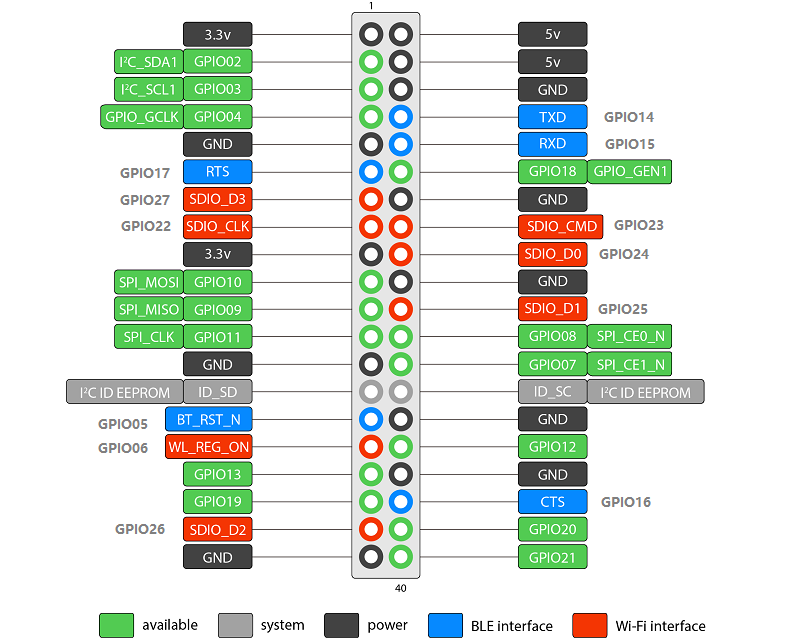
Anything in green is not needed, and as long as one Ground and one 5v (I already checked, the pHAT has it's own 3.3v regulator so doesn't need to tap 3.3v as well) all of the RED, GREY and BLUE pins need to connect. I know I want a few other interfaces made available (I2C, I2S etc) So let's see what the screen takes:
SPI: GPIO 7,8,9,10,11 also D/C on GPIO24 and RESET on GPIO25.
[looks at above pinout] all fine except 24 and 25... aww nuts. These are hardwired on the interface PCB. no problem, I'm had wiring the pHAT so I can just reassign SDIO to another alternative location with an overlay...
NOPE! SDIO only has one location on the main 40-pin header. There is an ALT on the full GPIO set on a Compute modue, but we're not using a compute module. Boo. I has a sad. which means..... BODGE WIRE TIME!
D/C and Reset are assignable to any free GPIO in the FPTFT driver, you simply set it as an option in commandline.txt so any of 12, 13, 19,20 and 21 are usable. So Lets go HACKING.
![]()
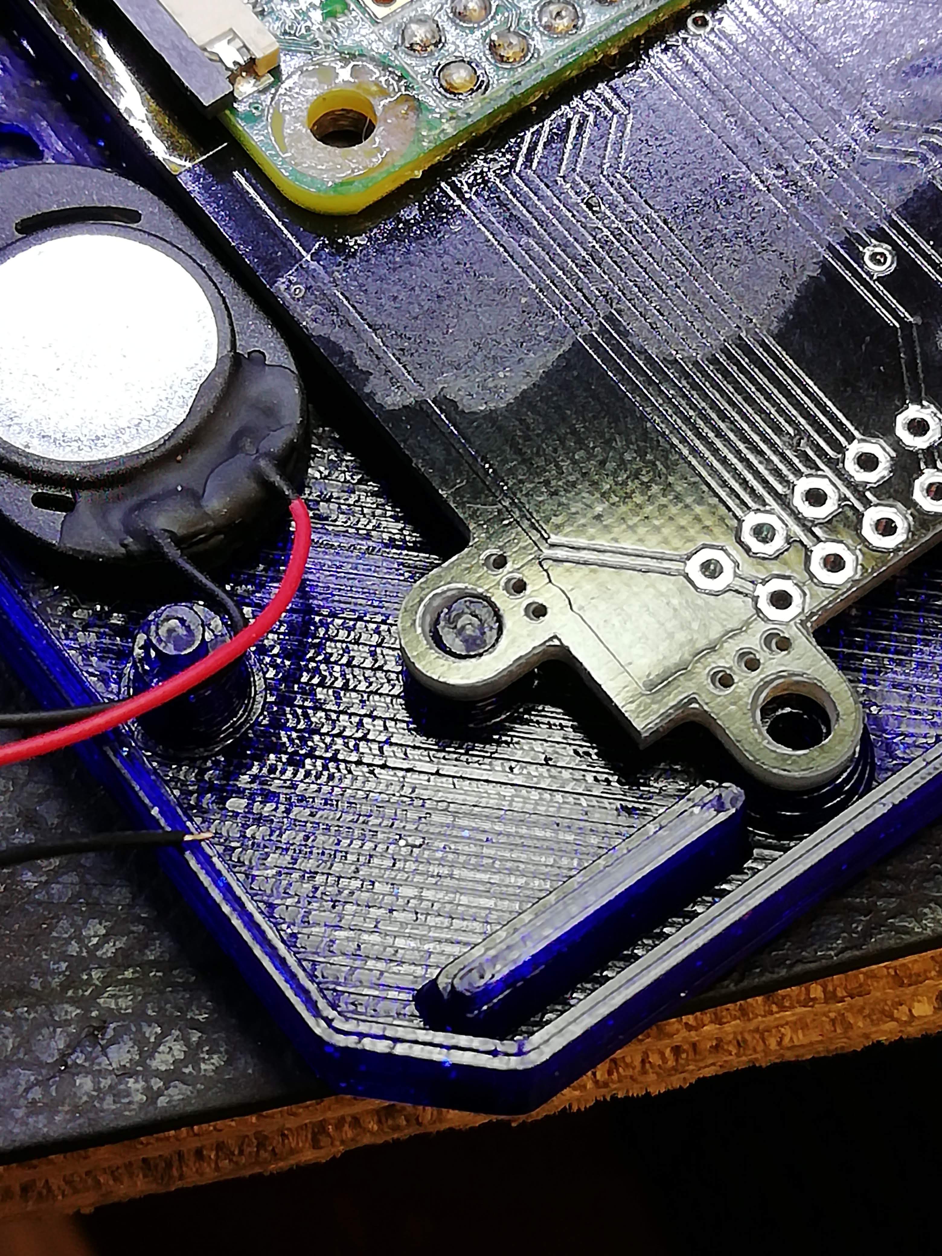
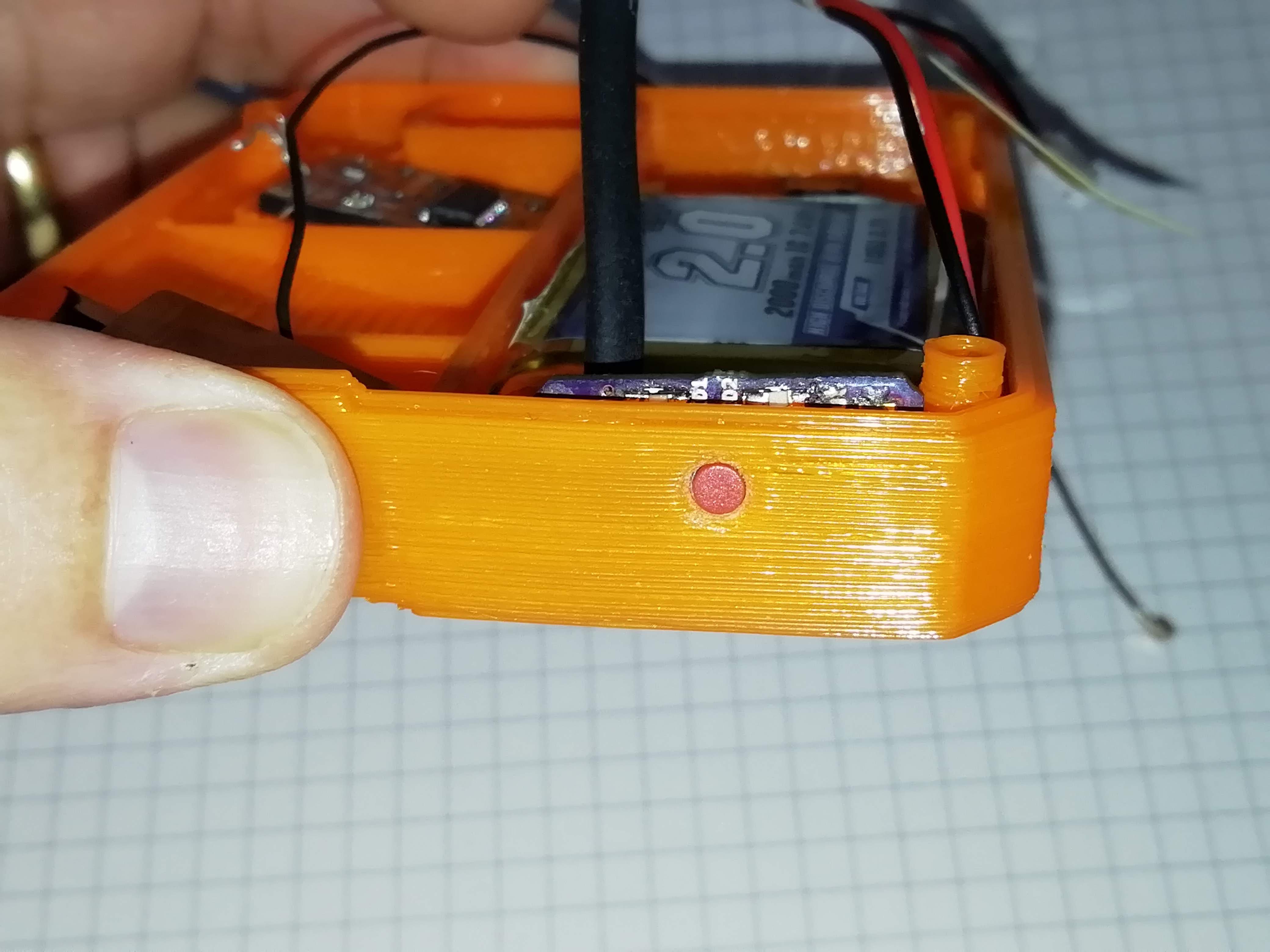
Just needed to cut 2 traces, solder some bodge wire from the pHAT to the DC/Reset Vias (blue wire) and direct solder to the DC/Reset points on the ribbon cable to their new GPIOS 20 and 21. then everything should JUST WORK (tm)...
But of course it's Hackaday, and no it didn't...
-
Testing the screen
10/09/2020 at 10:44 • 0 commentsHaving a nice case is all well and good but something needs to go in it. The competitions didn't need the deck to actually be built, but since the prize was a resin printed case, I felt I would need to build it anyway.
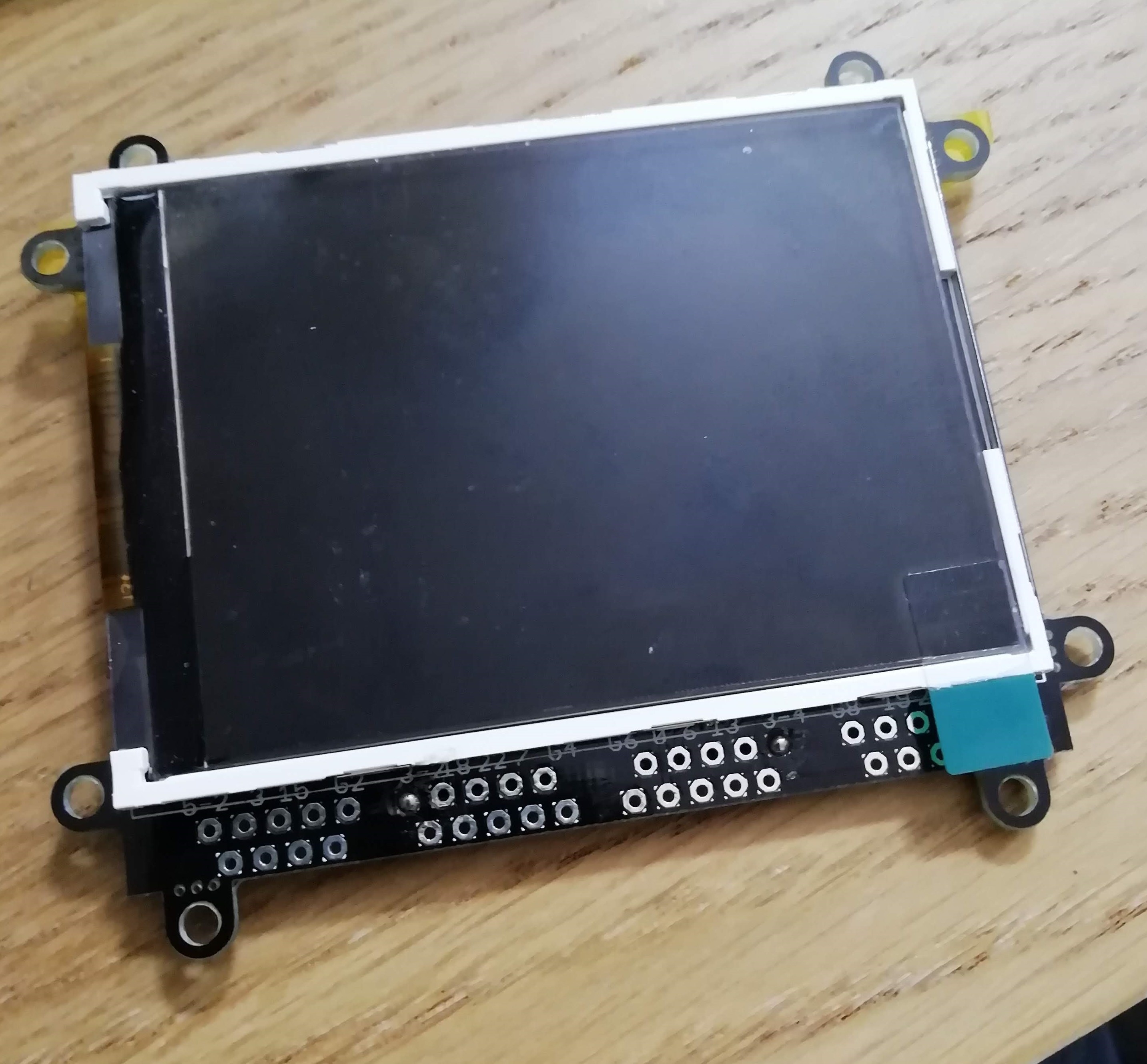
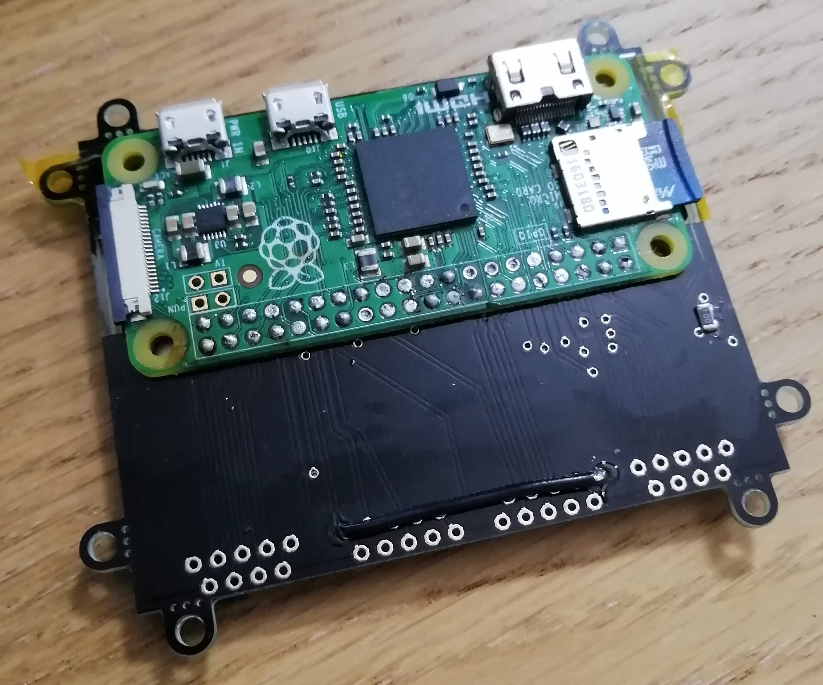
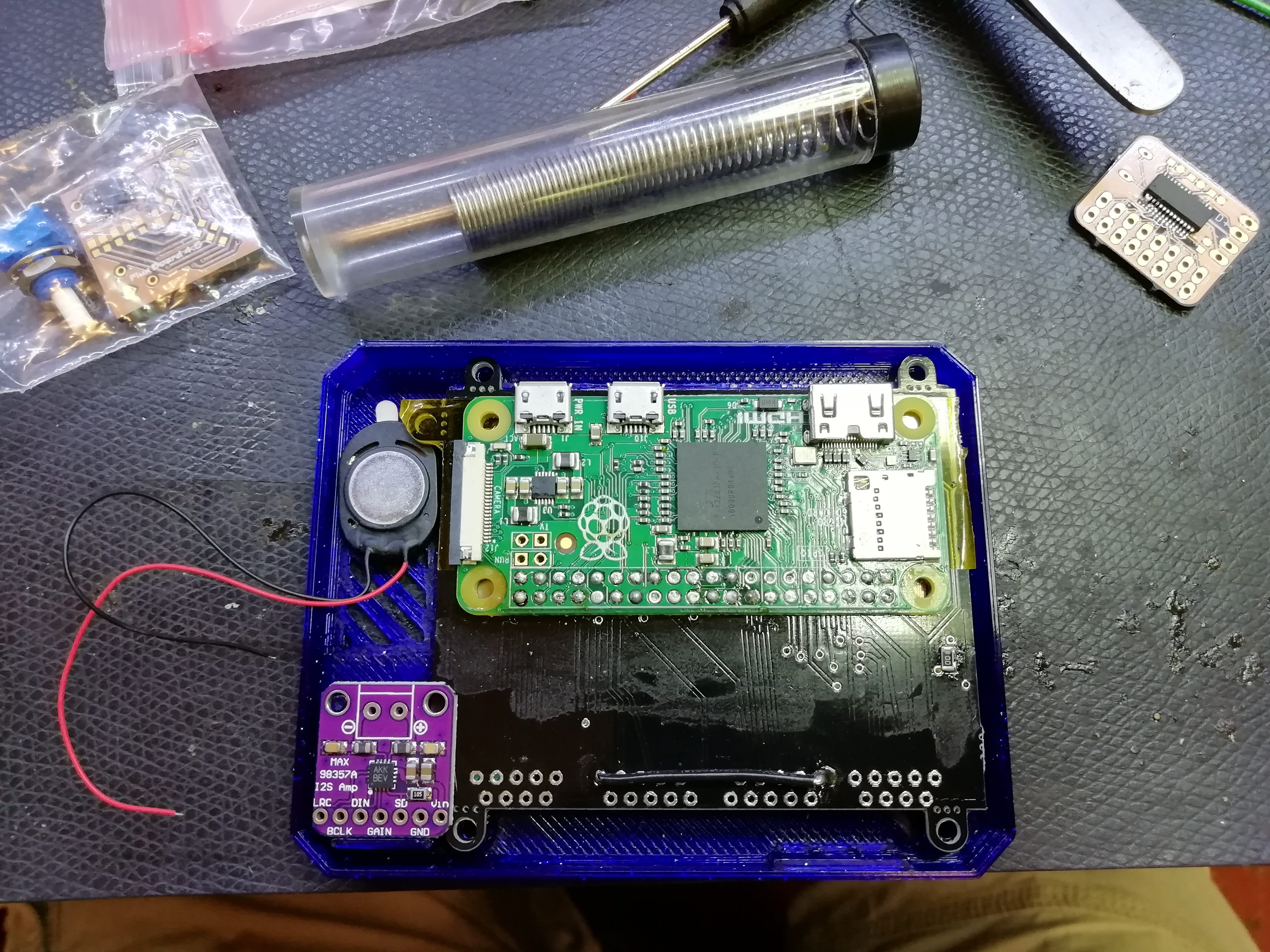
So to start with My Pi+TFT combo was already built, it just needed an OS setting up and would need the IoT pHAT setting up. should be simple, the pHAT has the eeprom for setting itself up on powerup. I'd just have to connect all the appropriate lines to the broken out pin headers on the TFT board.
![]()
![]()
They are not in the regular Pi connector 40-pin layout though so some hand wiring needed to be done. Just need to find which ones needed to be connected. No biggie.
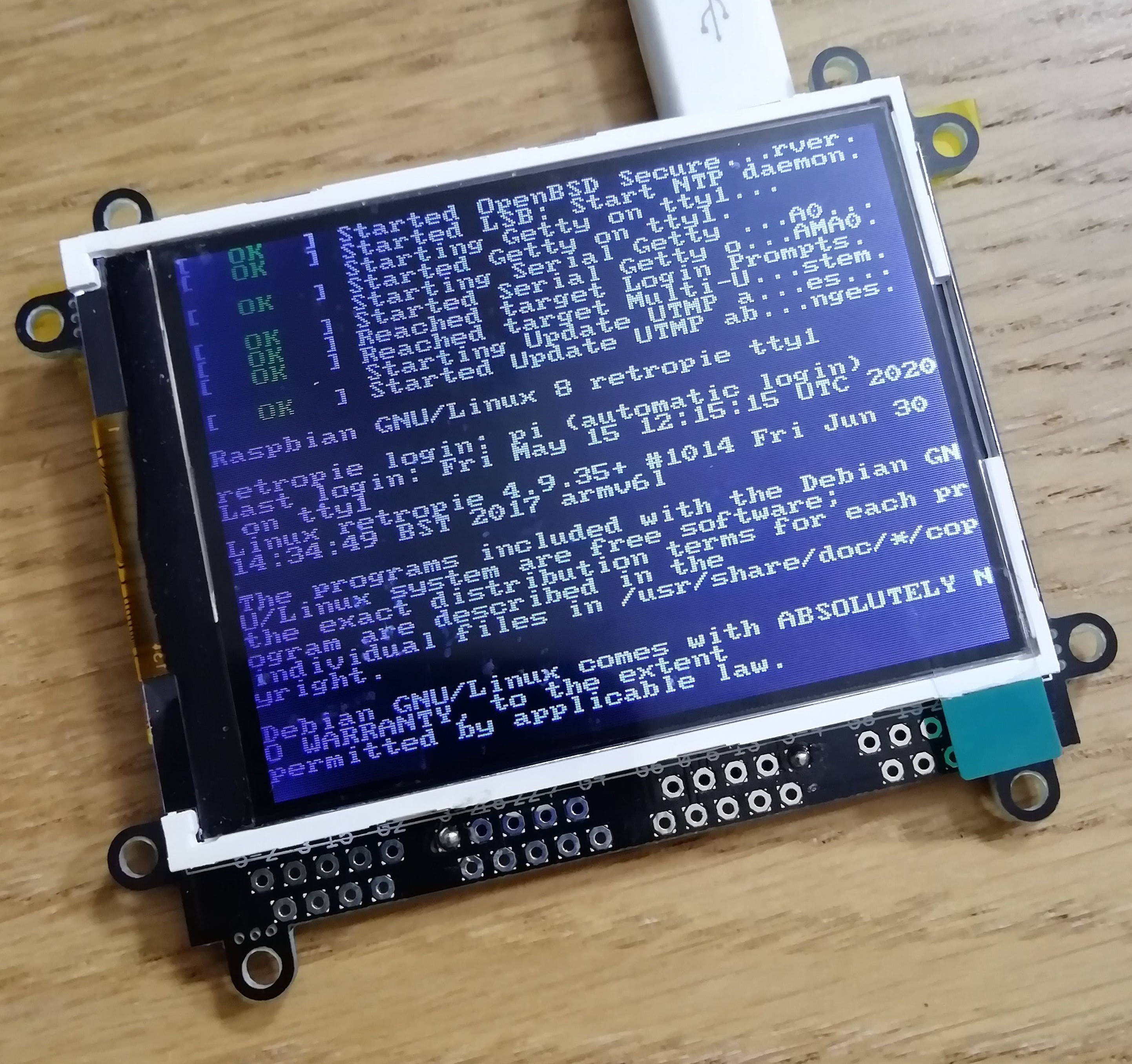
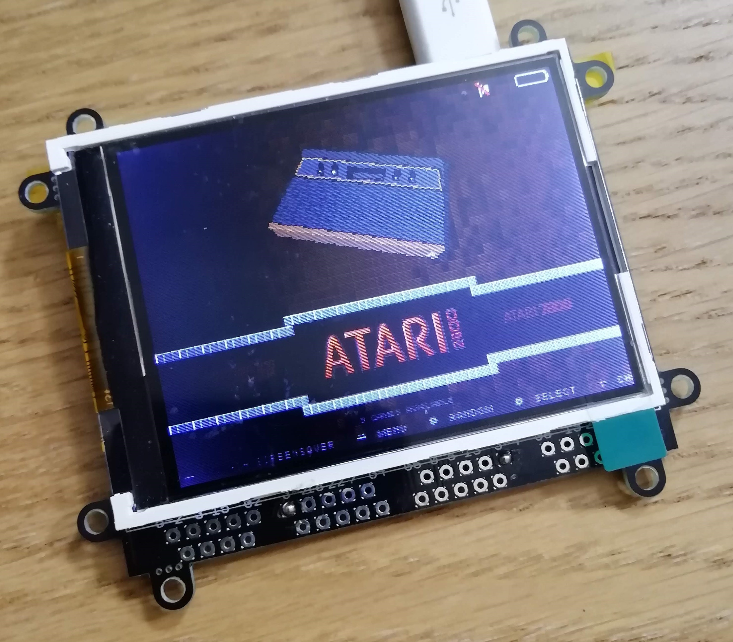
I yoinked an SD card from one of my other Pi's set up as a Gameboy Zero which has a similar SPI screen connected in an identical way so that I can test the screen still actually works.
![]()
![]() And WALLAH! So the pi and screen combo work. This uses an older Jessie based retropie install and the FBTFT driver with the same GPIO connections as Adafruit use for their SPI TFT's.
And WALLAH! So the pi and screen combo work. This uses an older Jessie based retropie install and the FBTFT driver with the same GPIO connections as Adafruit use for their SPI TFT's.
Now lets get to adding some devices. As this Pi has no WiFi connecting a keybaord and hub and transferring stuff via stick gets tedious quickly so lets get the pHAT attached.... Next -
Test Prints
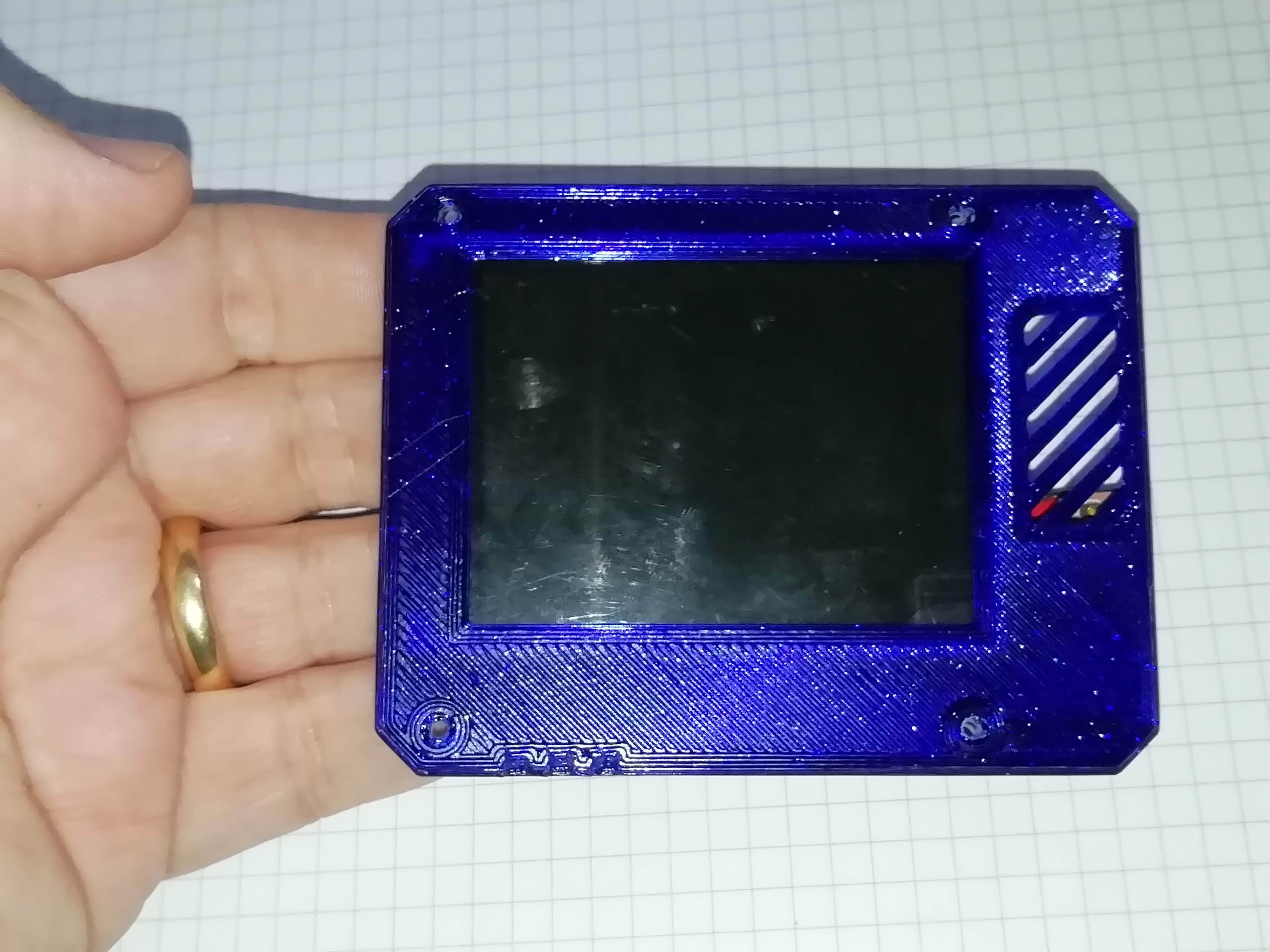
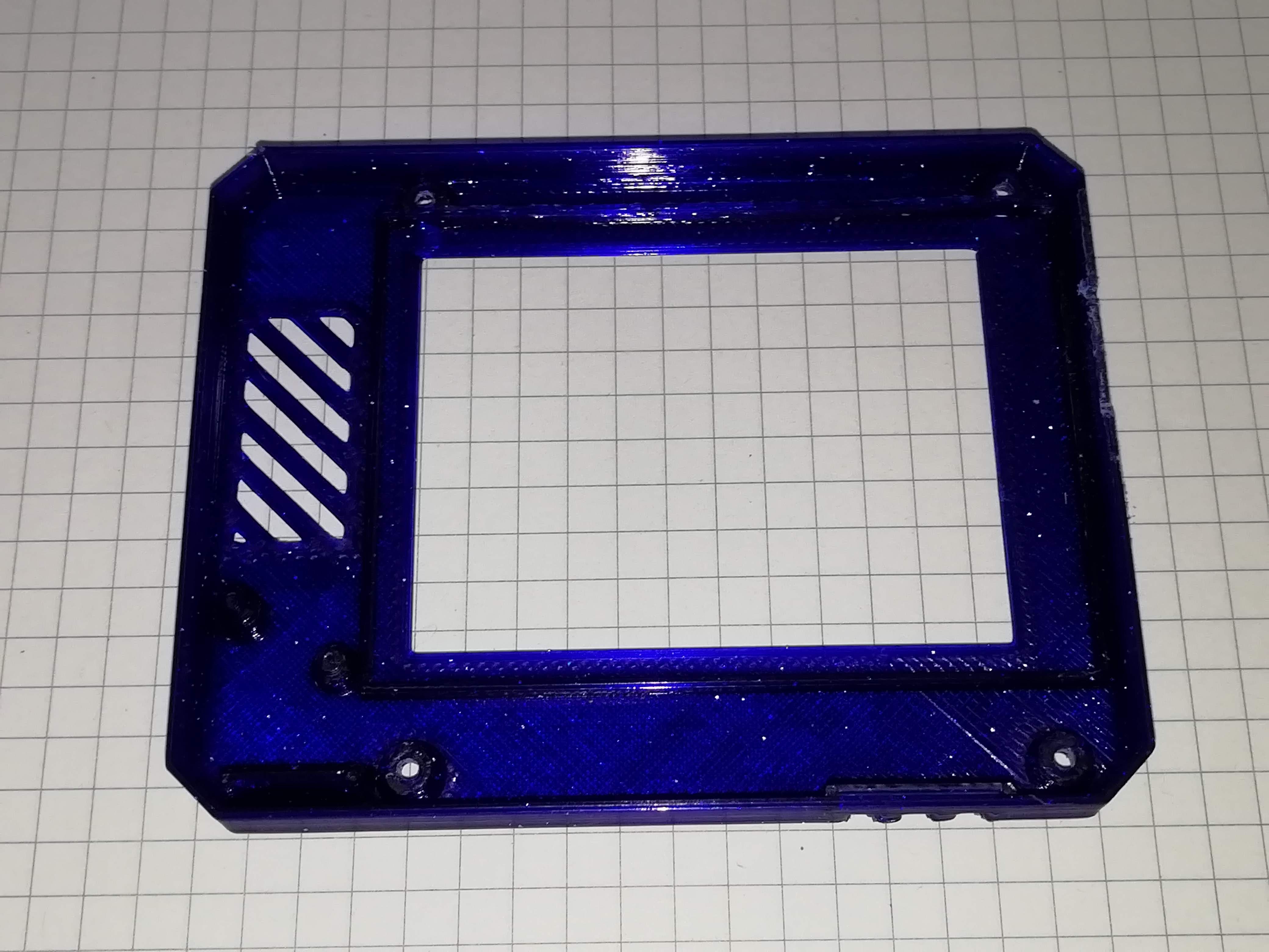
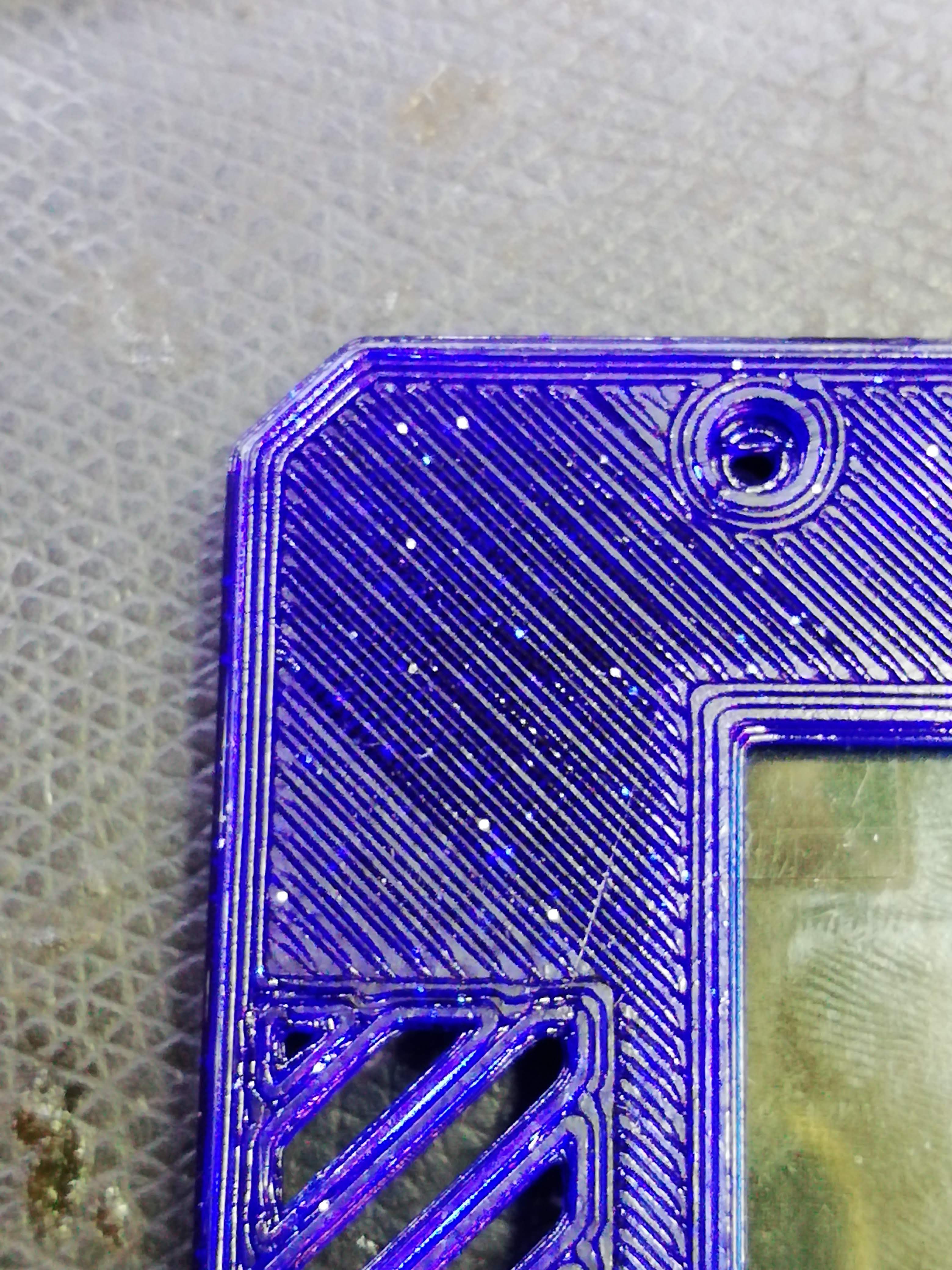
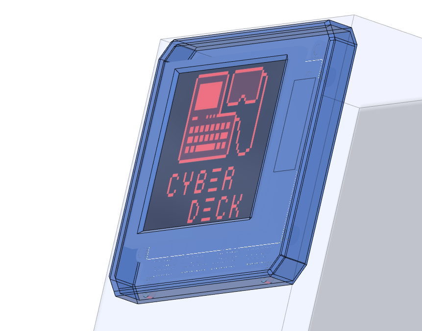
10/08/2020 at 15:49 • 0 commentsIn order to check the validity of my CAD modelling, I made a few low-detail 3D prints of the parts. There are various parts which have a built in tolerance adjustment that can be changed for either FDM or resin printing (important as the final part was to be able to be resin printed in the event that it won.) This was just set as a tolerance parameter and for FDM I used Noe Ruiz's recommendation of 0.2mm for FDM.
![]()
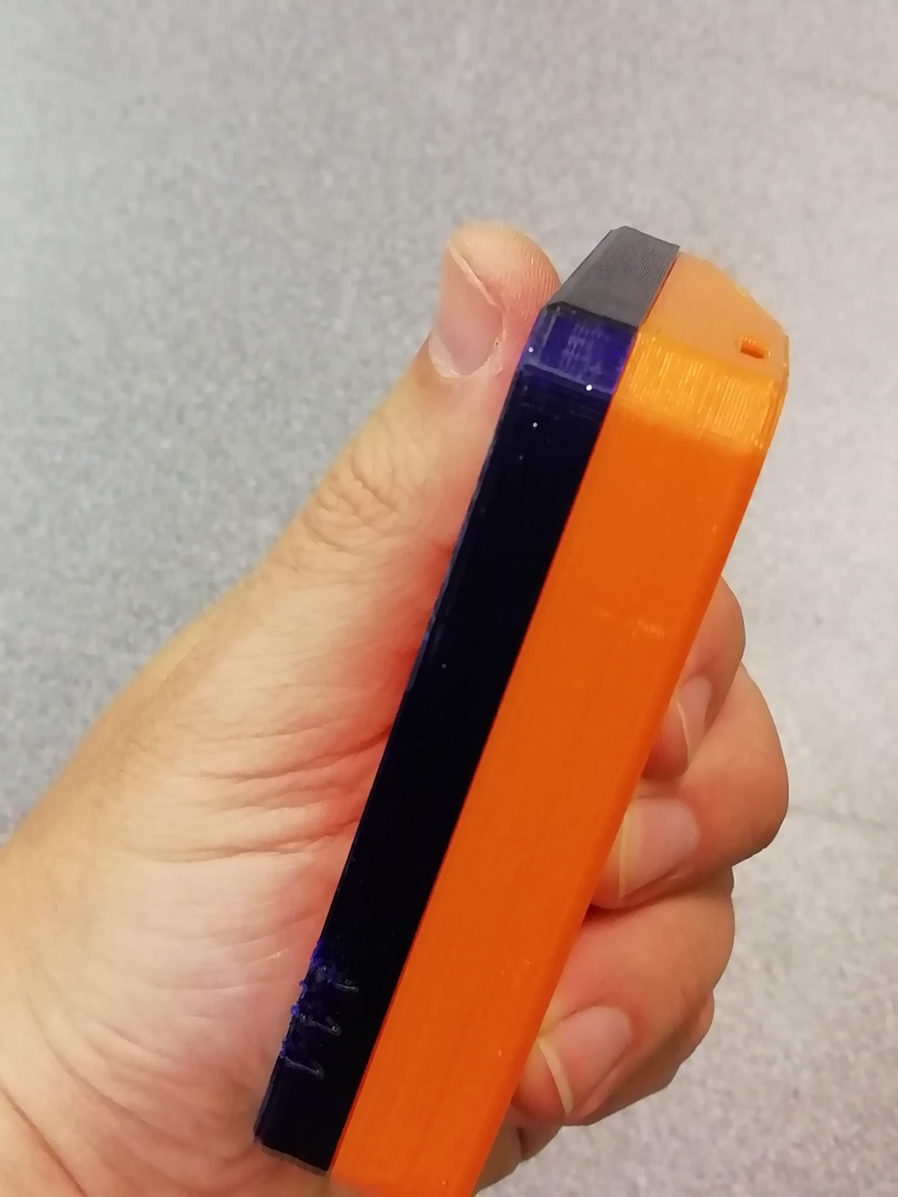
Looks like a great fit but one of the sides was 1mm off so could be easily corrected in CAD
![]()
![]()
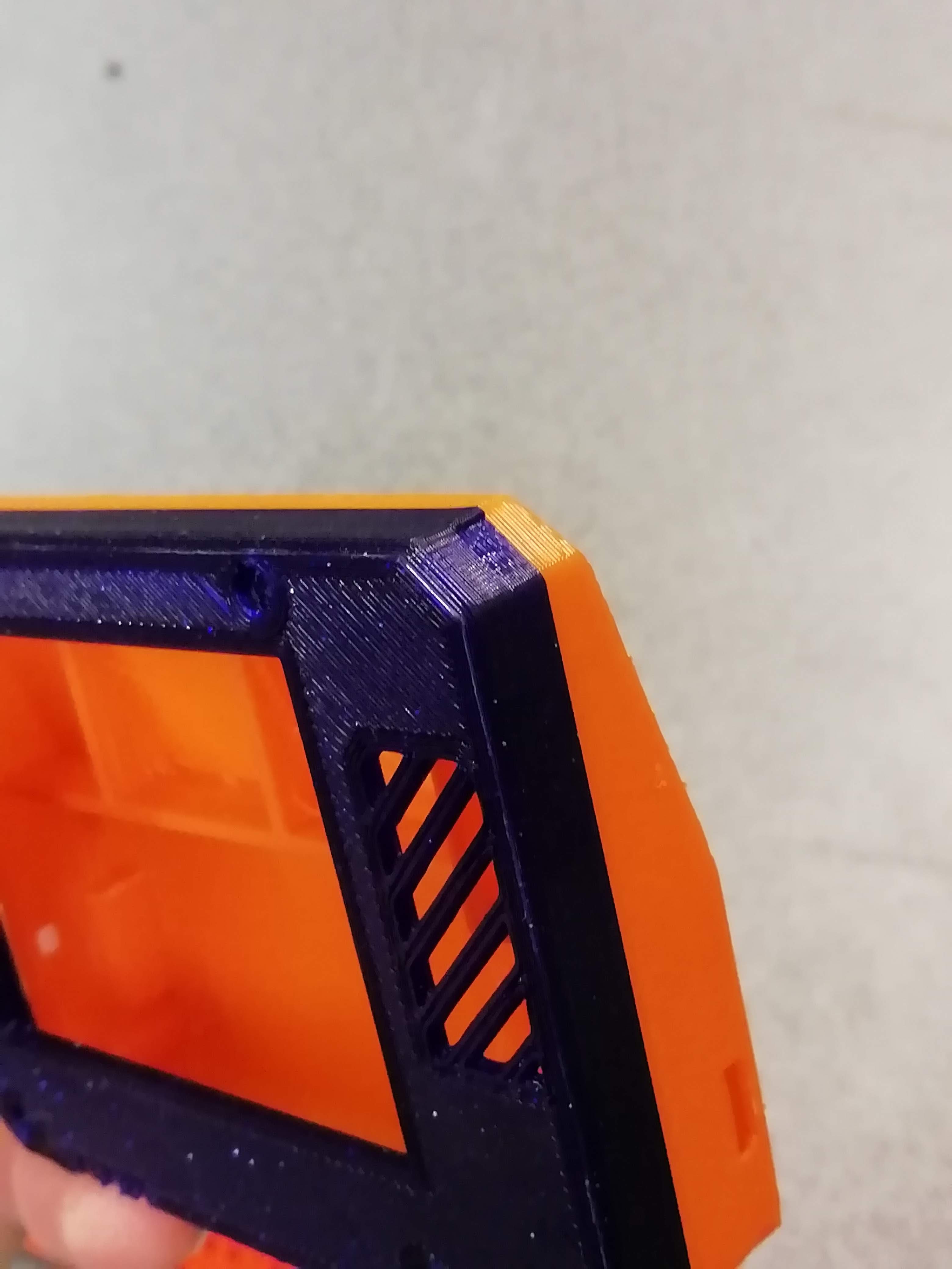
The colours are't final, just what was loaded up, but dayum! that sparkly blue...
![]()
![]()
I'll take that as a first pass!
And for the rear case:
![]()
![]()
![]()
![]()
All looks really good!
![]()
![]()
And fits together well too! There are a few minor changes to make but that's why we make test prints...
-
CAD - Designing the case
10/07/2020 at 23:23 • 0 commentsHaving got the basic shape sussed out and the specific component parts I was going to use, it was time to start getting the the main case sketched out in Fusion.
![]()
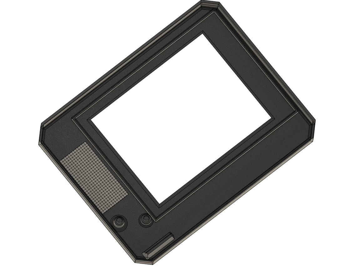
The front part of the case was created by simply extruding a rectangle somewhat arbitrarily bigger than the screen PCB (the tabs are sticking out of the side but in real life I've snapped those off) then chamfering the corners and front edge then finally shelling out the inside to a 1mm shell thickness.
![]()
![]()
Once the basic shape was formed, internal detail for mounting the boards could be made. Having accurate representations of the parts means I can just place them where I want and project sketches from them to form mount turrets and ledges by extrusion and drafting.
![]()
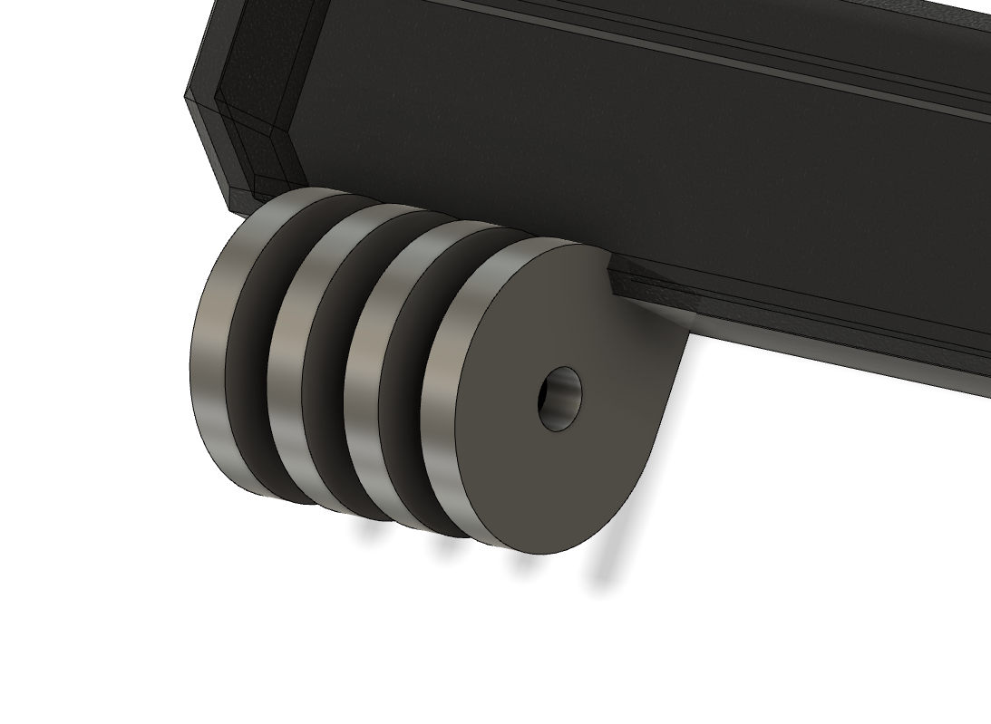
The hinge was made with an ofset plane, with a circle sketch and additional lines to connect it to the main body. the part was then multiplied with an array to bring out the GoPro mount style hinge
![]()
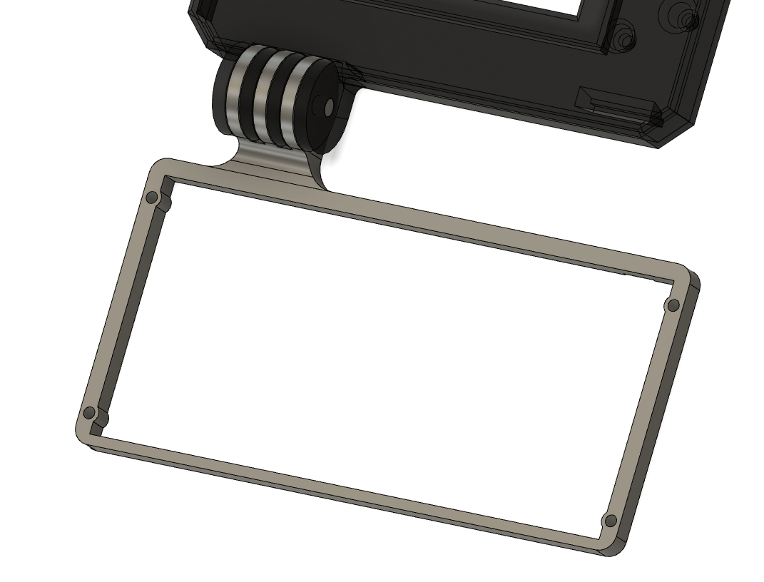
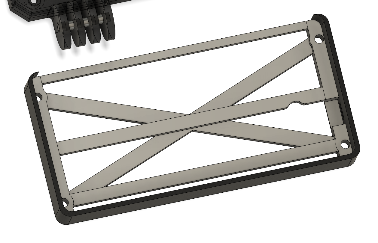
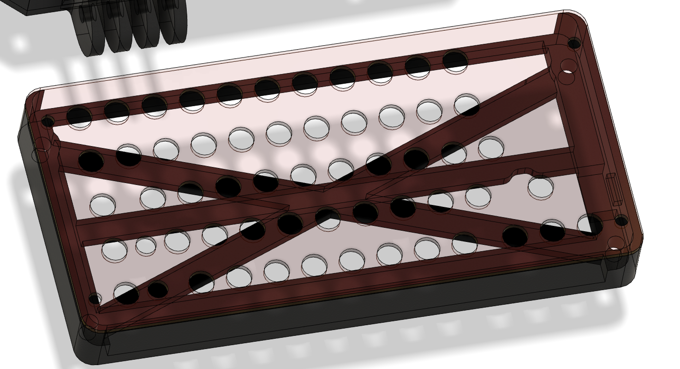
with the hinge created, a matching lower half can be made using projections from the Keyboard PCB to make a spacer thick enough to sit the top PCB piece above the tact switches
![]()
followed by a lower frame to both hold screws that are going to come in from the top face plate and protect the underside electronics (and hand from the through hole pins of the tact switches)
![]()
From the top plate PCB I projected the holes to make a sketch for a laser-cut top-top-plate. (more on this later as the reasoning behind it was completely a stylistic choice.
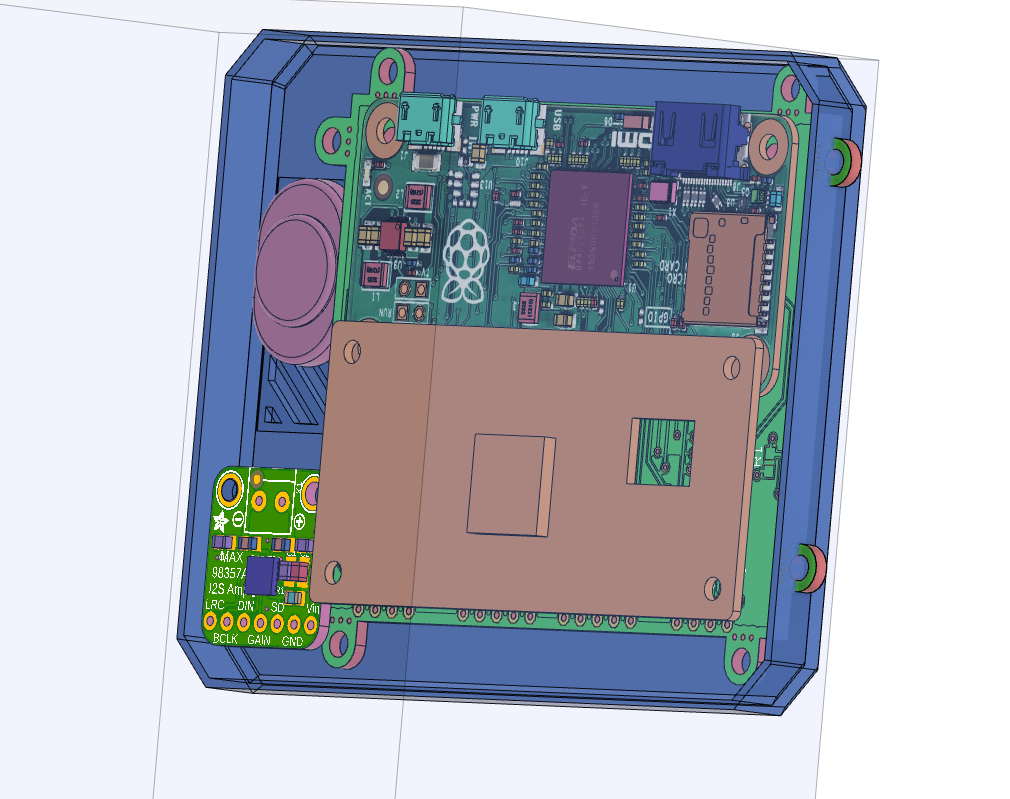
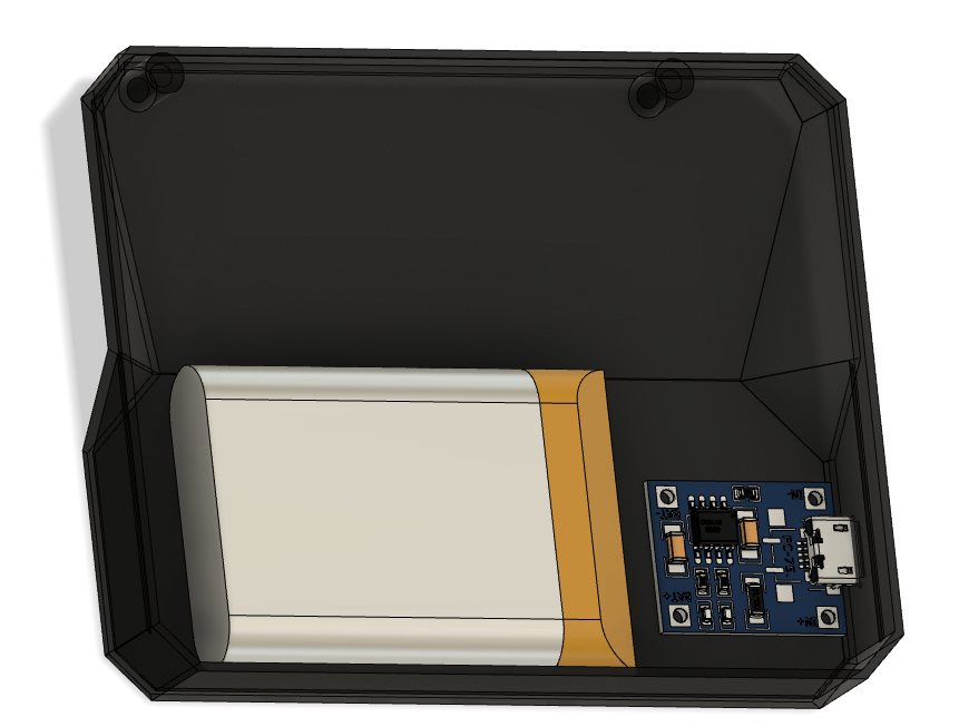
Now I could fill out the back part of the case. the front was already pretty full, with the screen, Pi, WiFi HAT, audio DAC USB hub and speaker aperture, but I still had to get a battery, charger, and a soft on/off button board into the case.
![]()
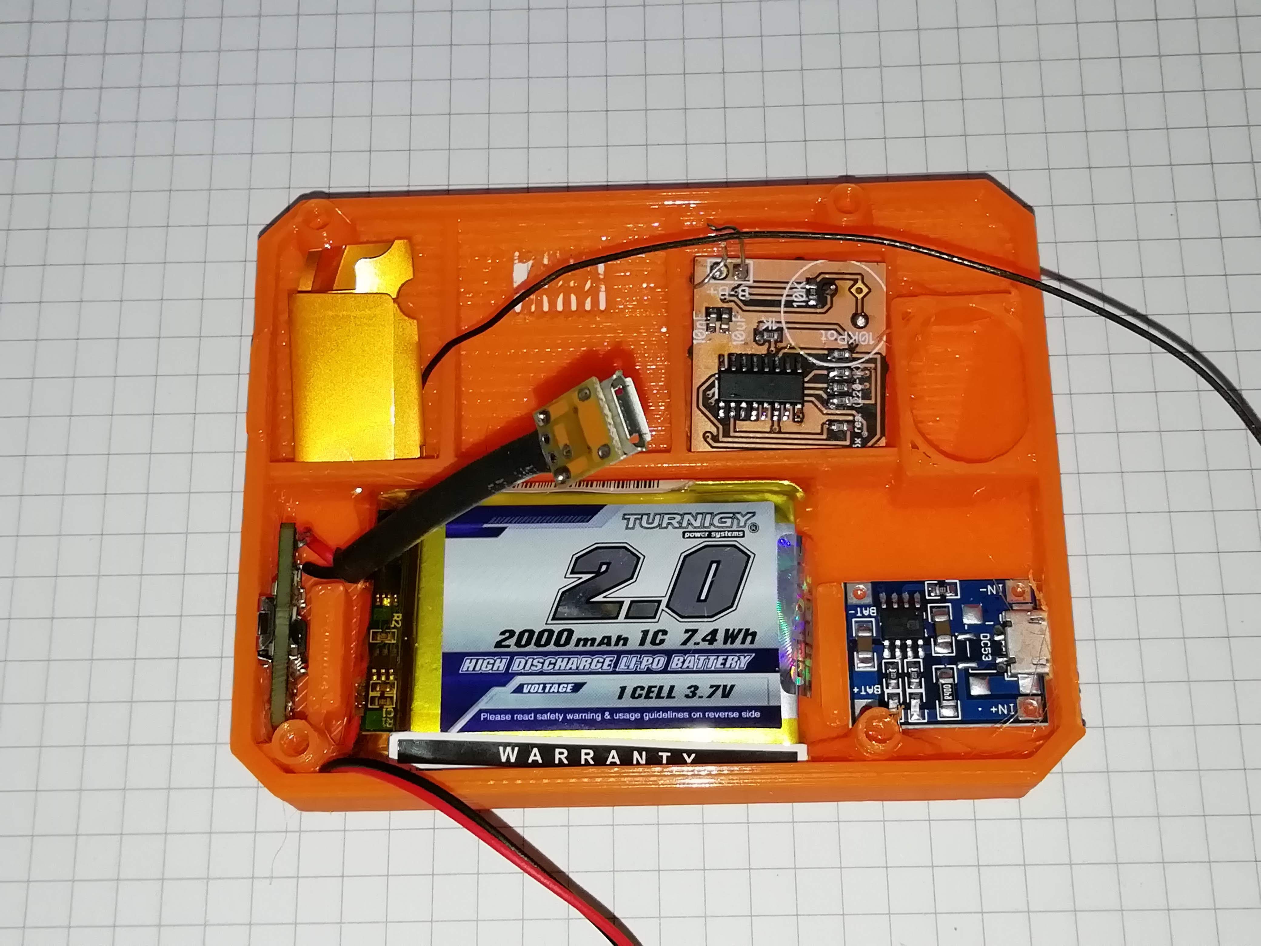
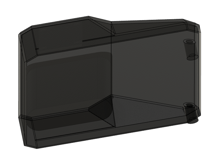
I started off with an extruded rectangle chamfered to match the front case but had to extend to fit in the THICC battery I had spare. I didn't want just a block hanging off the back of the case so pulled some draft angles and somehow ended up with something not too dis-similar to an Argon40 Pi case...
![]() Next update... Test prints
Next update... Test prints -
CAD Design - Capture internal components
10/07/2020 at 13:28 • 0 commentsAfter recent successful forays into using Fusion 360 I wanted to use this project to further extend my skills and keeping Adafruit's Layer by Layer playlist on hand I was ready to do that. So first I'd need to accurately capture my internal components before I could figure out where they would all go and make mounting points for them.
Any PCB's that were designed in KiCAD can be exported as a STEP file and thus can be directly imported into Fusion. providing that KiCAD has the component models installed too. otherwise it will export the bare board. Anything designed in EagleCAD can have .brd files imported into Fusion as it has Eagle baked right into it. in both cases if major components are missing from the import, the can be easily added from component generators or librabies such as Grab CAD. Where this was the case, I mostly just imported major components like IC's, connectors and other tall things like crystal cans, while skipping small SMD resistors etc.
Finally, any boards I didn't have access to design files I just modelled as close as possible the old fashioned way with calipers and CAD sketches.
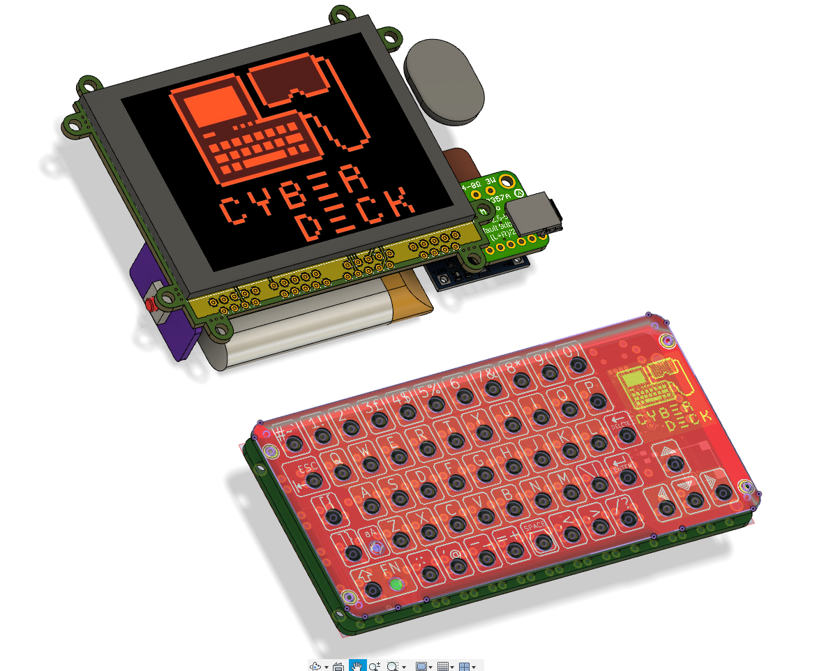
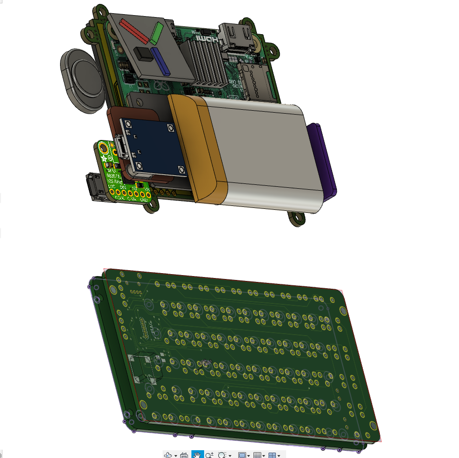
Here's the components as laid out in their final positions.
![]()
![]()
Obviously I haven't added in connection wiring so is something I need to be mindful of when I place components. The chosen battery is 2000 mAh with a 1c discharge rate or 2A so my power footprint is limited by that, though I don't intend to go anywhere near that anyway. Which means my heaviest wire needs to be 26AWG and most can be 28 or 30AWG.
-
Initial Design
10/06/2020 at 09:48 • 0 commentsWith the main components selected it was time to work out what direction to go in, as there was limited time to work on this. A month sounds a lot but that's only 8 available sessions at the hackerspace (SoMakeIt in Southampton, UK) and a few other evenings to work on this. Time was tight so I had to crack on and get something roughed out in order to not flail around wasting time in CAD.
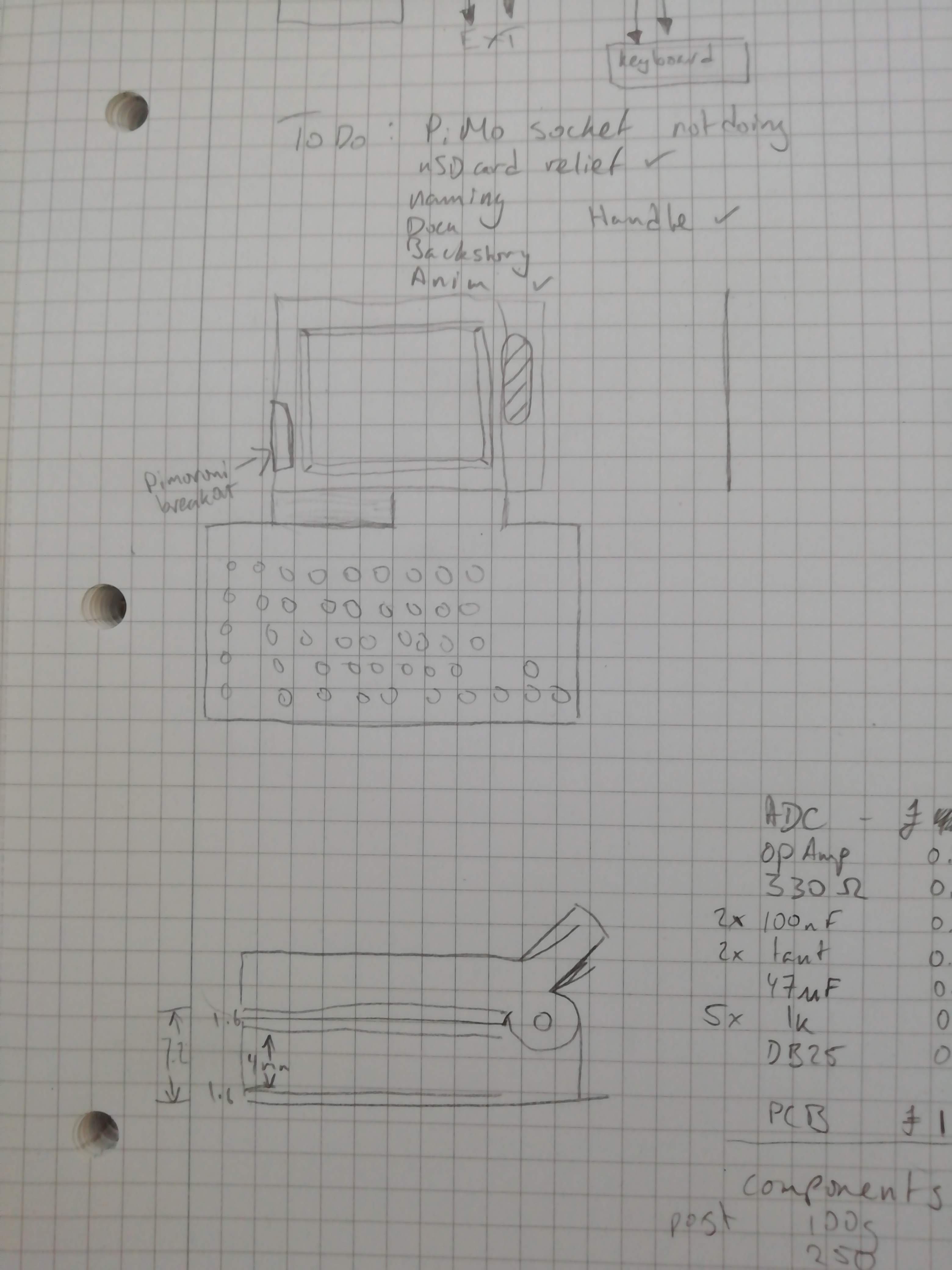
My initial thought was something clamshell like a Gameboy Advance SP and since all the weight was going to be in the "screen" part, then it would need a kickstand or something. Since I also wanted a handle I thought to combine the two and sketched out this:
![]() It's not pretty but gives the basic concepts of what I'm building. I just now had to fit all this into it:
It's not pretty but gives the basic concepts of what I'm building. I just now had to fit all this into it:![]()
-
That bobricius keyboard
10/05/2020 at 12:59 • 0 commentsCustomizing [bobricius]'s design
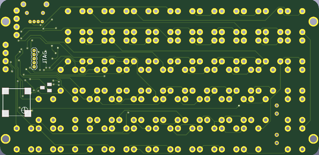
When I got the design file for the mini PiQwerty keyboard off [bobricius]'s project page it was an eagle .brd file and just to sanity check it, uploaded it to OSHPark but it didn't have any traces routed. I thought this was strange since in his logs he talks about the firmware working or not... So I imported it into KiCAD and got to work routing the board myself (only to later find his github repo with a fully routed board :picard_facepalm: )
![]()
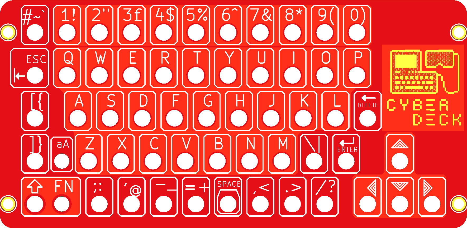
Also while I was in there, imported the Cyberdeck logo designed by [BillieRuben] and popped it in a suitable place before shipping the design off to JLC.
![]()
With the speed JLC was turning around in and getting the PCB's to the UK around the end of August I thought there was plenty of time to get one built for the competition...
What a mistaka ta maka
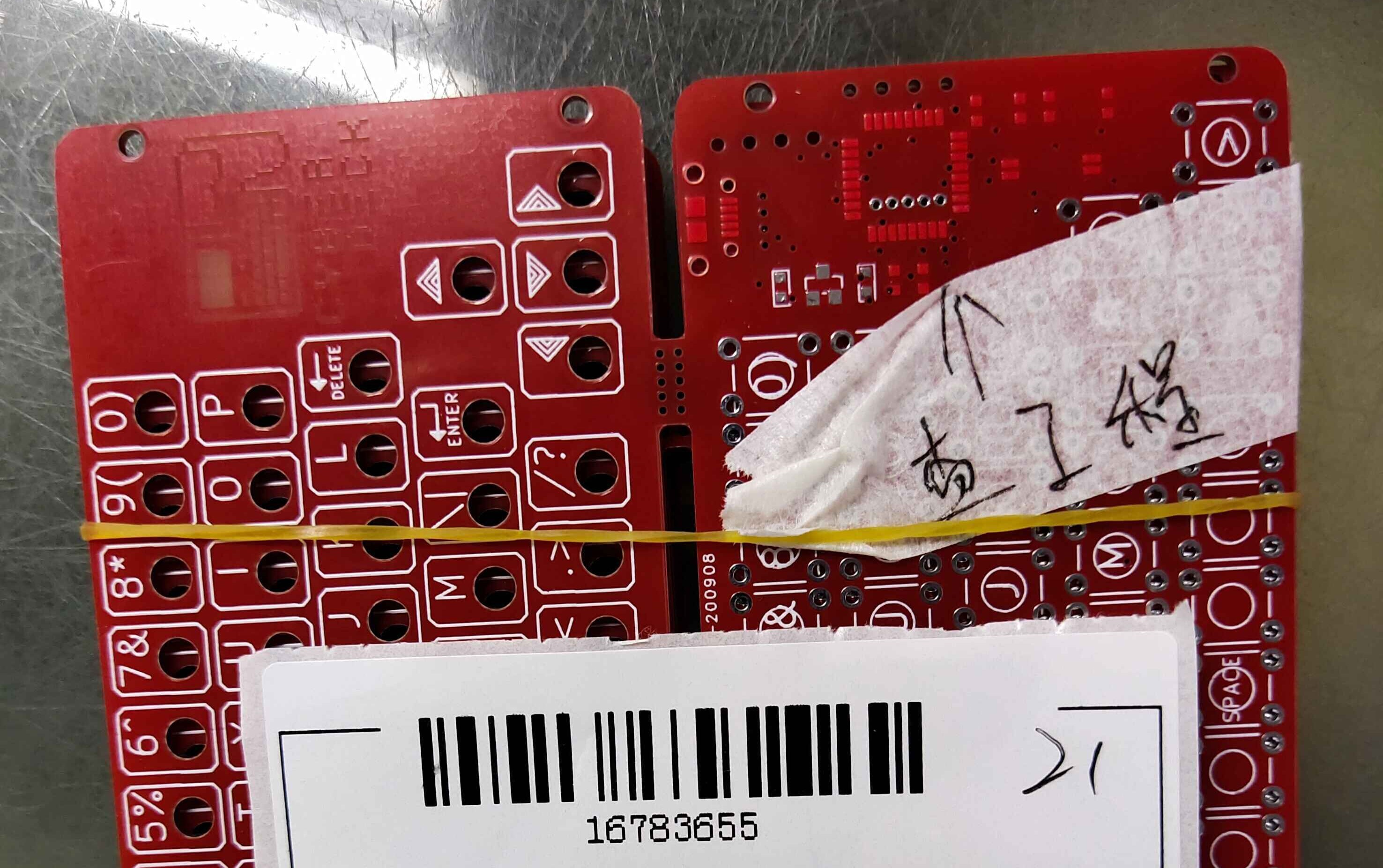
I followed the process of the boards going through production as JLC does and was expecting a shipment notification when I received an email asking if I'd intended for there to be no traces on the board. AT ALL.
WHAAAAAAA?????
![]()
Importing Eagle .brd into KiCAD
So it turns out when you import an eagle .brd file into KiCAD, it sets the copper layer names to be the same as they were in eagle, but leaves the rest with KiCAD defaults. Then when you plot gerbers, the gerber files have this mish-mash of layer names. The file headers are correct so when you load them into gerber viewers everything is hunky dory. This includes the JLC (and many others - so I'm told) upload previewer.
However the software they use to ACTUALLY PROCESS the board is not so intelligent and can't cope with the mixed-up layer names. So my copper layers vanished. I only discovered this by uploading the gerbers to OSHPark which DOES give you a real preview before comitting to produce the board, and threw a warning that there were no copper layers in my submission.
So I did eventually get my boards but not before the end of the competition. Oh well... building the deck is not a competition goal as it's a design comp, just a nice to have and probably earns bonus points in the unknown judging criteria.
-
First step - pick main components
10/04/2020 at 22:31 • 0 commentsScreen and Wifi
On the announcement of the zerodays competition I thought about what I had in my spares box that i'd be able to use and a dormant PiCB-TFT which already had a zero attached was staring me in the face waiting for it's time in the sun.
![]()
![]()
So that was pi and screen sorted. I had batteries a-plenty and chargers from bulk-buys from other projects, but the pi was a non-W variant so would need wireless to make it a true cyberdeck. Fortunately another board I had lying around was a redbear IoT pHAT. A wifi and bluetooth board that came from when there were no integrated wireless Pi's available that I backed as a kickstarter project (though are sadly no longer available) and never found a use for before the zero-W was released.
Keyboard
So I only needed a few other bits to make a funtional deck. The main part would be a keyboard and most decks use a mini bluetooth keyboard, but my inspiriation came from the N-O-D-E youtube channel and his latest zero-terminal V3. Featuring a tiny PCB+tact switch keyboard that according to the notes was a variant of a design by [bobricius] which I found here and that seemed a perfect fit.
Sundries
The final pieces of the puzzle are sound (a MAX98357A I2S DAC and AMP in one board from Adafruit and a 14x20mm speaker from my bits box) a USB hub (4 port retrocution board from OSHPark) and a LED flux capacitor (also from OSHPark by SwedishVaper) for some blinkenlights
So now all I had to do was design the sucker....
PlagueStation Zero
An entry into the cyberdeck.cafe zerodays deck design competition
 ABrugsch


 And WALLAH! So the pi and screen combo work. This uses an older Jessie based retropie install and the FBTFT driver with the same GPIO connections as Adafruit use for their SPI TFT's.
 Next update... Test prints
 It's not pretty but gives the basic concepts of what I'm building. I just now had to fit all this into it:
