 Frédérik Berthiaume
PLEASE NOTE : there is an oversight in my PCB design : DDC112 digital pins are 5V, and the TinyFPGA are 3.3V and are NOT 5V tolerant (it's a bit not clear on the internet, but the ICE40LP8K specs don't mention 5V anywhere). I'm just lucky my poor TinyFPGA survived this treatment and I hope everything's fine. So it may be ok to use it that way, but be warned! It should be easy to add a logic converter and I definitively will if I ever put some time in this project in the future.
0%
0%
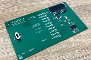
Picoammeter
A device to measure very, very small electric currents, based on DDC112 analog front end
Become a Hackaday.io member
Already have an account? Log in.
Just one more thing
To make the experience fit your profile, pick a username and tell us what interests you.
Pick an awesome username
hackaday.io/
Your profile's URL: hackaday.io/username. Max 25 alphanumeric characters.
Pick a few interests
Projects that share your interests
People that share your interests

 Clyne
Clyne
Here are my learning experiences with DDC118:
https://hackaday.io/project/2042-the-optical-inch/log/51162-pcb-clean-up-and-endianness
Call me paranoid, but if you want good results, you'll need shielding and chassis GND that is separate from circuit GND. I ended up adding eight u.fl connectors to the board and it appeared that connecting the shields of all cables on both sides wasn't good enough. That is, it looked like floating the sensor-side ground and adding another shielded can around the PIN diodes (with the shield connected with Cu braid back to the board) made a difference.
If you're looking to build measuring equipment, I'd suggest either sleeving coax with metal braid, or going straight to triaxial connectors altogether. RP-TNC connectors are somewhat affordable, as they're used for WiFi / antenna gear.
Keithley / Tektronix have "low triboelectric effect" triaxial cables for the 2450 / 2470 SMU series, but that's probably where I'd draw the line. The antenna cables one can buy should be just fine as long as they're not moving around and the temperature is allowed to stabilize.