 Joel Kozikowski
How Photo Etching works:
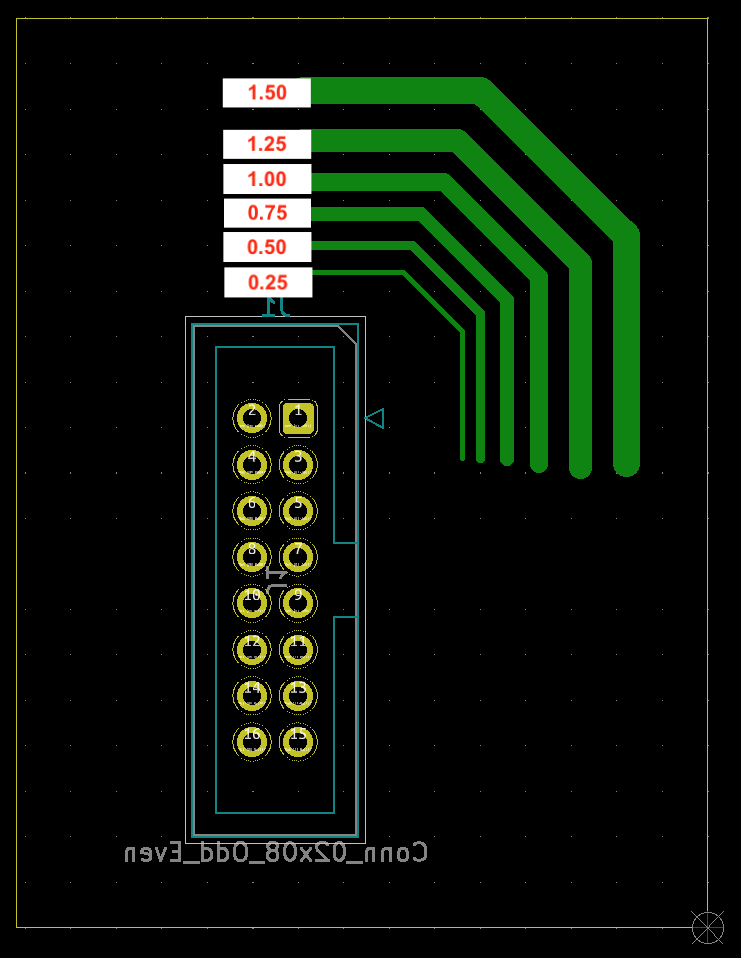
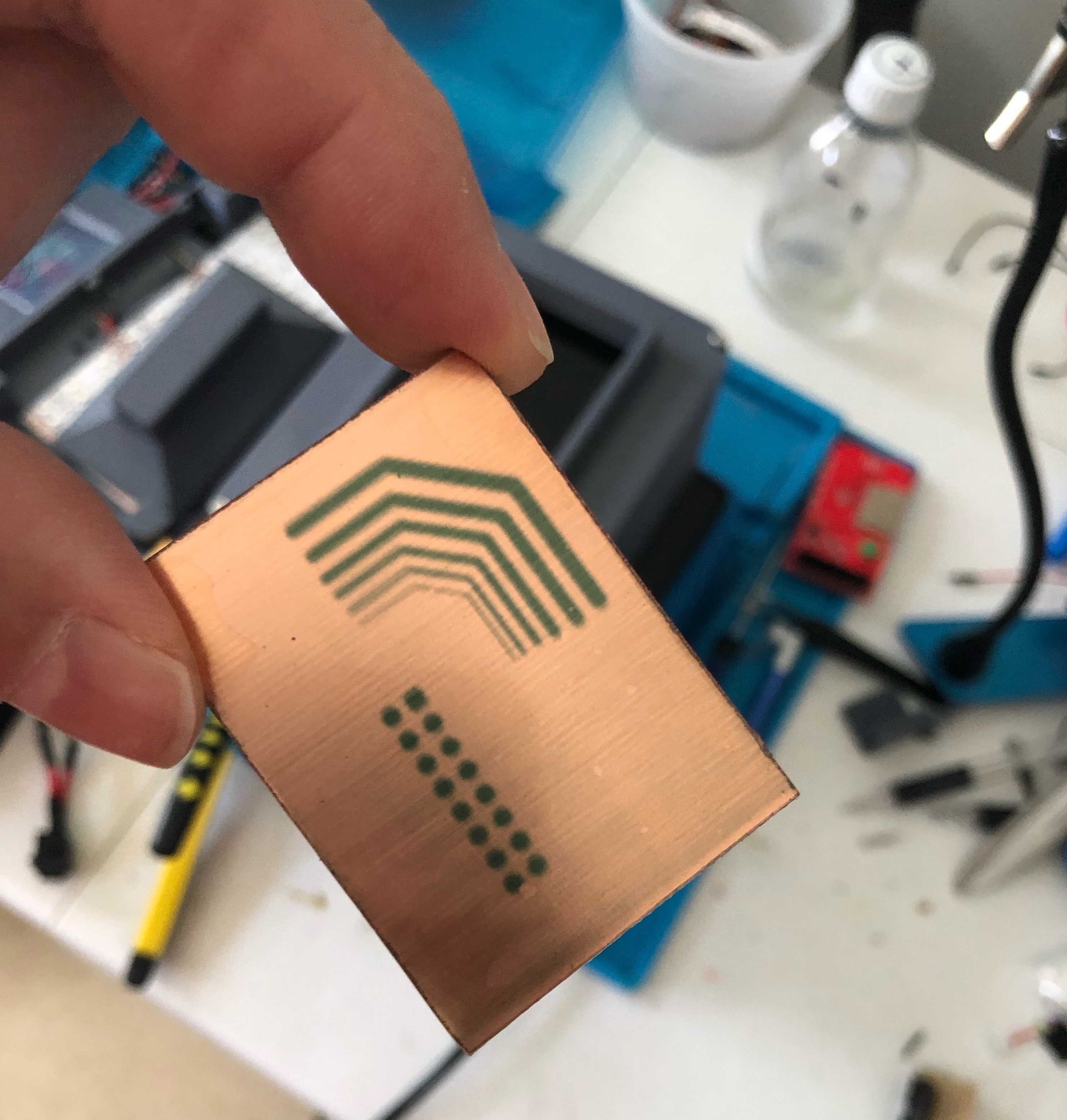
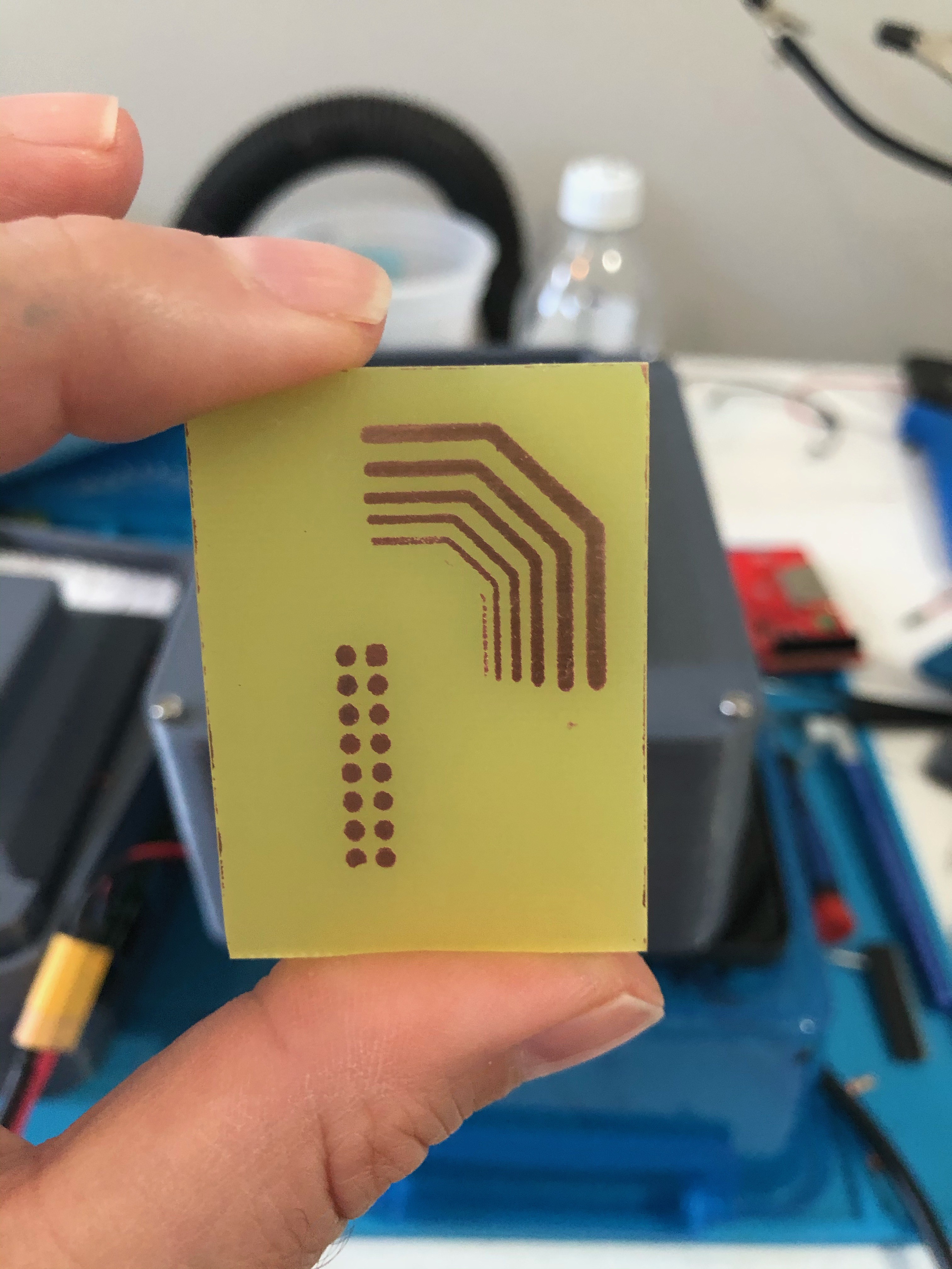
The unit is designed to facilitate "photo etching" of copper boards. "Etching" a PCB is done by protecting the copper that represents the traces with an "etch resistant" coating. The board is then placed in an etchant like Ferric Chloride, where the copper that is not covered with etch resist is chemically disolved away. What remains are the copper traces. Qwicktrace works with various "photosensitive copper boards", where the "etch resist" of the traces is made in one of two ways:
- Expose the traces to UV light, which strengthens the etch resist, making the copper underneath the exposed area slower to eat away. This allows the non-trace area to be removed first, leaving the traces behind.
- Hide the traces from UV light, which weakens the etch resist on the rest of the board. The board is placed in a "developer" chemical that eats away UV exposed etch resist, leaving behind the entire copper clad board, but with traces still covered by the resistant. The board is then placed in the same etchant in step #1, where the non protected copper is eaten away.
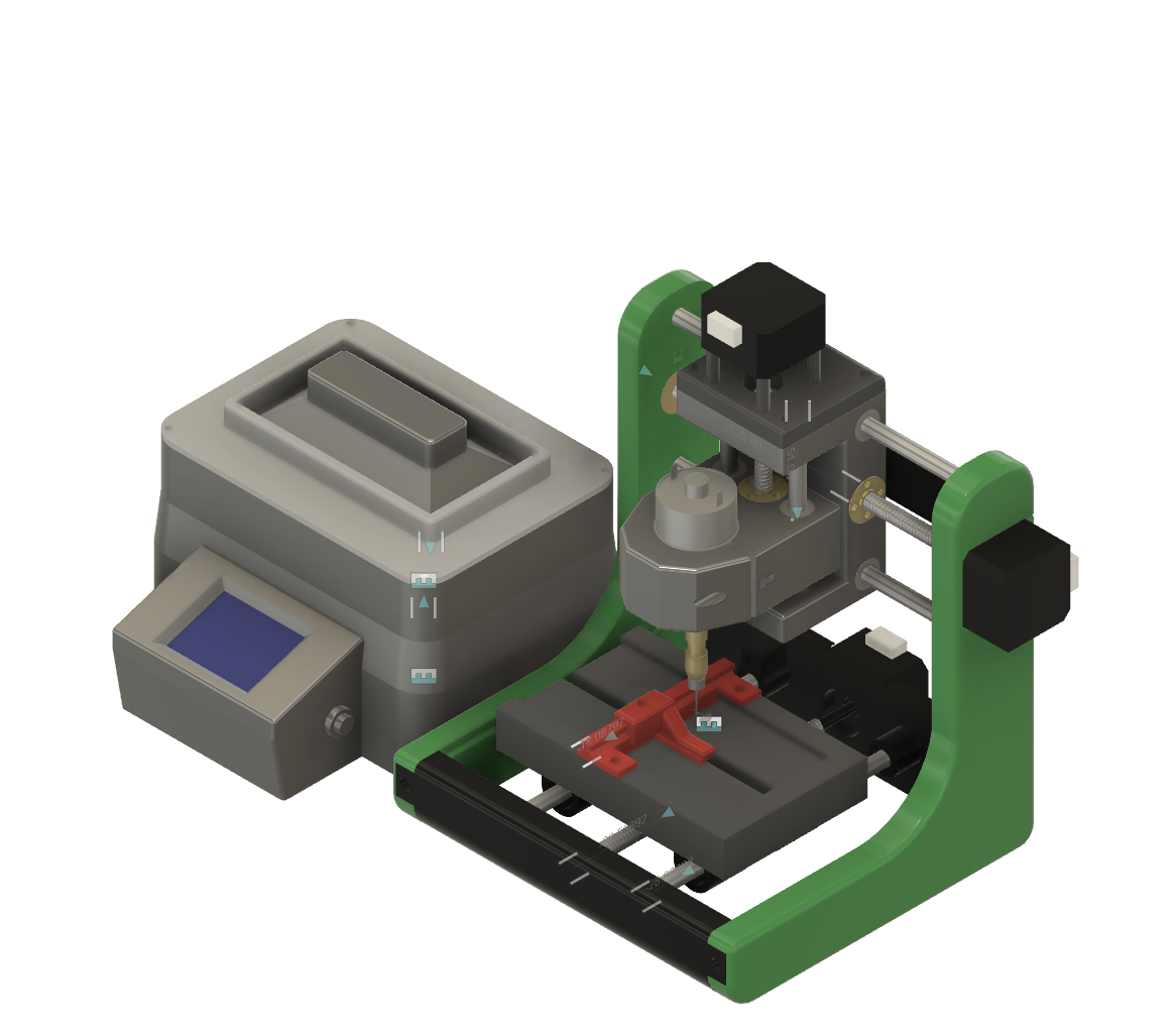
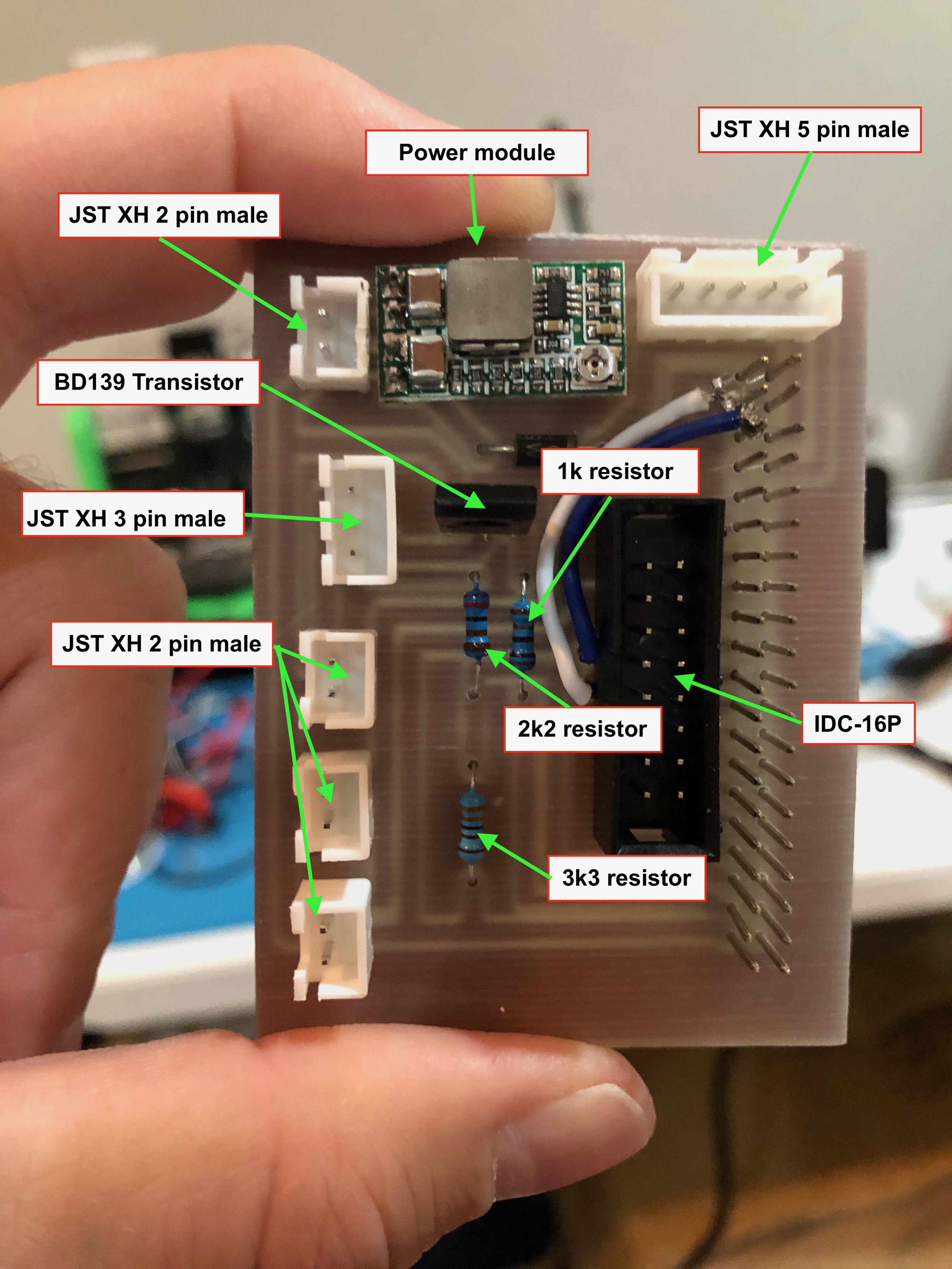
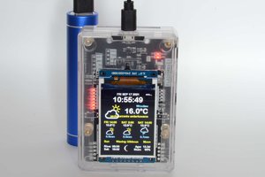
How Qwicktrace PCB works:
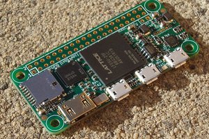
The Raspberry Pi 4 controls the unit, including the small TFT touchscreen used for the user interface. A simple custom "Hat" PCB fits onto the Pi to help it out with controlling the various components. The Qwicktrace software understands how to read and render Gerber files and SVG files, so the process of using the unit is as follows:
- Upload a Gbr or SVG file to the unit's "pcb-files" directory
- Select the file you uploaded on the unit's touch screen. Files are listed in reverse date order (most recent on top).
- Select a "profile" used to expose the photosenstive copper board. The profile determines whether the UV light reaches the traces or the non-traced area, as well as the total exposure time needed.
- The Qwicktrace unit renders the circuit traces as either a negative or positive image, turns on the UV LEDs to expose the board, then turns off the board when exposure is complete.
The LEDs run on 24 volts, but their on/off state is controlled by the Pi via a PWM on a GPIO pin that is connected to the lamp's LED controller IC. The Pi and the HDMI interface board both require 5 volts, which is supplied by the small voltage regulator module on the Pi Hat. The Rev 2 board of the Pi Hat uses a "stackable header pin connector", which has extra long pins, and allows the GPIO pins of the Pi to be exposed and connected to even with the PiHat board in place (for future expansion).


 Valentin Angelovski
 Josh Kittle
 andriy.malyshenko
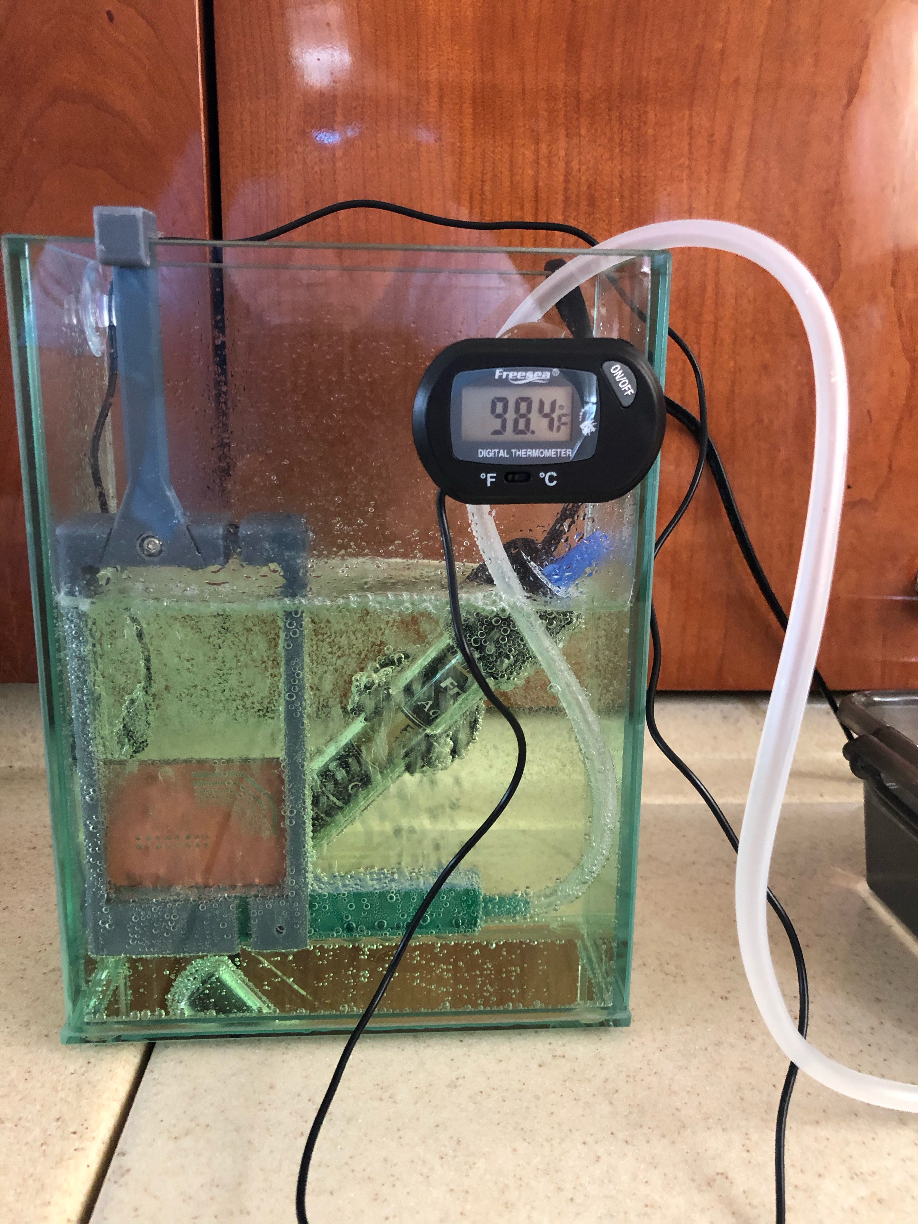
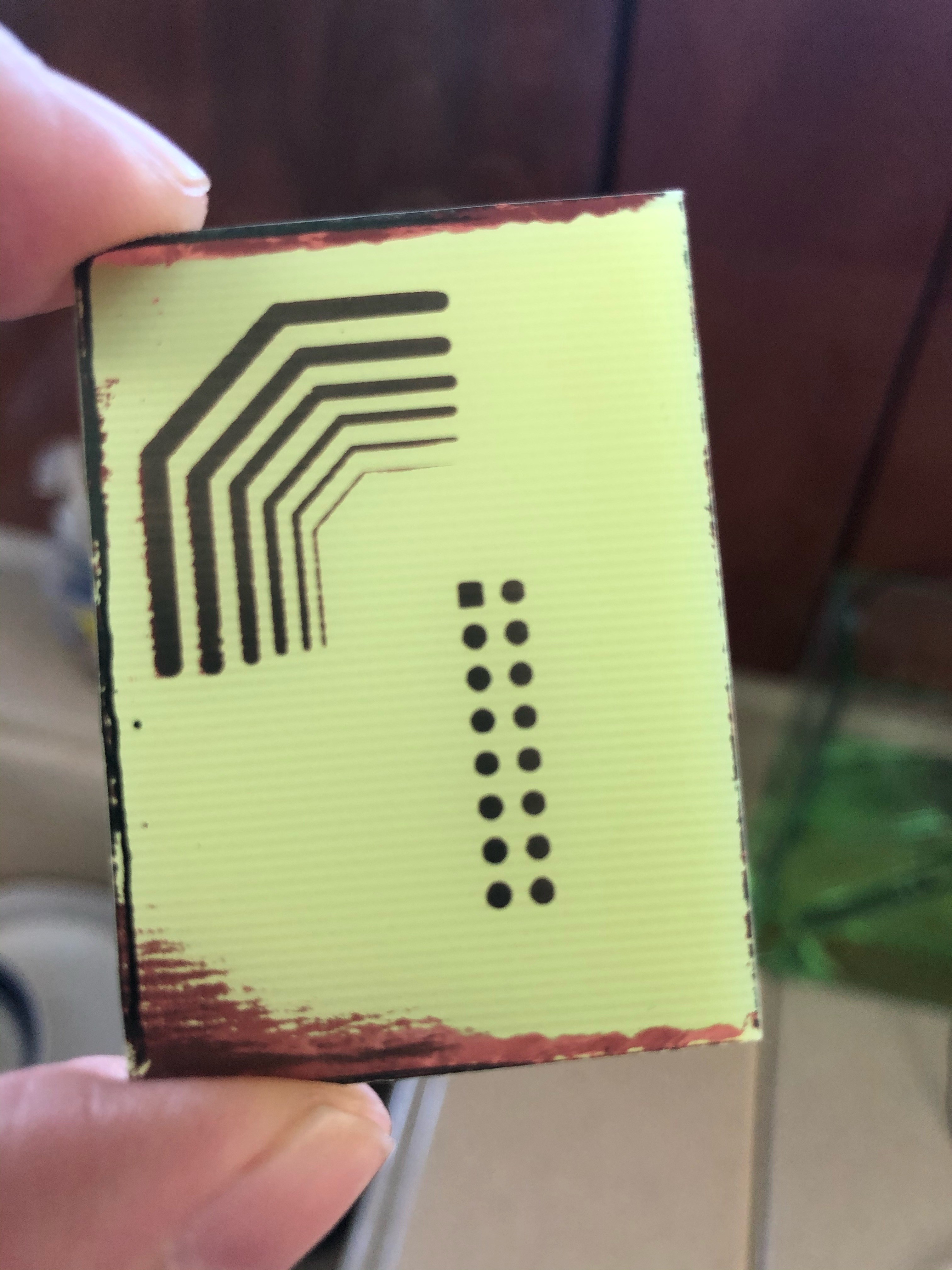
I jerryrigged the same LCD + a random 50W UV lamp from amazon together. I was able to expose 0.2mm traces, double sided. I aligned the two side manually on the edge of the LCD itself. I used the same corner of the PCB. I simply aligned the masks on the opposite edges of the LCD to achieve that. It was really easy to align. A proper case would add some corner bracket for a perfectly repeatable alignment. I found you also need enough weight on the PCB to keep it flat against the LCD. I did use the LCD upside down. To reduce the parallax. I was surprised by the quality of the result. I don't think my UV light is supposed to send the light rays parallel.
There is one thing odd though. If I put a piece of photoresist front of the UV light, it takes 10 seconds to fully expose it. But through the LCD it takes 15 minutes! That seems excessive. Its cooking the hell out of the LCD itself. Is it some sort of UV wavelength mismatch? How are MSLA printers doing it in few seconds?
edit: pictures of a the successful test. The hardest part is applying the photoresist film. I didn't do a good job.
https://ibb.co/xJt13fb
https://ibb.co/ggKt293