 Aleksa
Now that the FPGA code was done, I could finally assemble and test the whole system. There were many untested blocks at this point, so each block was tested incrementally to pinpoint any issues. Once these incremental tests were done, the final test would be hooking up a signal to the front end and getting the sampled signal data back to the host PC.
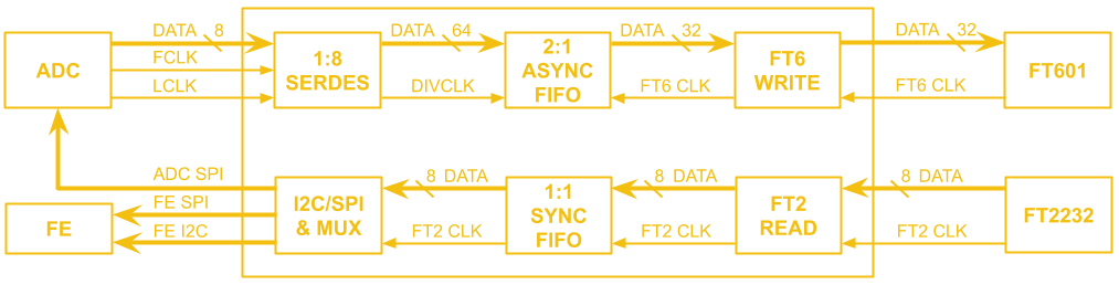
The first of the incremental tests I did on the system was to turn a relay on in the front end. This would confirm that the FT2232 chip as well as the FT2 Read interface, FIFO and I2C FPGA blocks were working correctly. I figured out which bytes to send based off of the IO expander IC's datasheet and made a quick python script using pyserial to send the data (this interface on the FT2232 looks like a serial port to the PC). I executed the script and heard the clack of the relay on the front end board, it worked!
Next up, I would send a SPI command to the ADC to come out of power down mode. The ADC clock starts running when it goes into active mode, so I programmed the FPGA to blink the LEDs if it gets a clock from the ADC. This would confirm that the SPI FPGA block and ADC board worked. Some more datasheet searching and a new line of python later, I was greeted with a well-deserved light show from the (too-bright) LEDs on the digital interface board.
I tested the maximum transfer rate next. To do this, I lowered the clock generator's frequency from 400 MHz (theoretical maximum throughput of the FT601) down until the FIFO full flag (which I tied to an LED for this test) was not set while running transfers using FTDI's Data Streamer Application. This resulted in a consistent data throughput of 370 MB/s. This also verified that the FT6 Write block was initiating transfers correctly when the requests came in from the host PC.
Up to this point, I didn't check the actual data coming in, only that the transfers were happening. I enlisted the help of a more software-savvy classmate (this scope would become our capstone project in a later term) to modify the data streamer code to dump a csv file from the data received. I then set the ADC to output a ramp test pattern. Since this pattern was generated inside the ADC, it would test only the FPGA blocks and not the front end. I captured the data and got what i expected: a count up from 0 to 255 and back to 0, over and over again. I did a basic check through the file and found no missing counts, this meant the transfers were completing smoothly with no interruptions in the FIFO or in the USB interface.
Finally, I hooked up my function generator to the front end, got together the set of commands needed to start sampling and sent them to the ADC. This would be the final test, a real signal in and sampled data out.
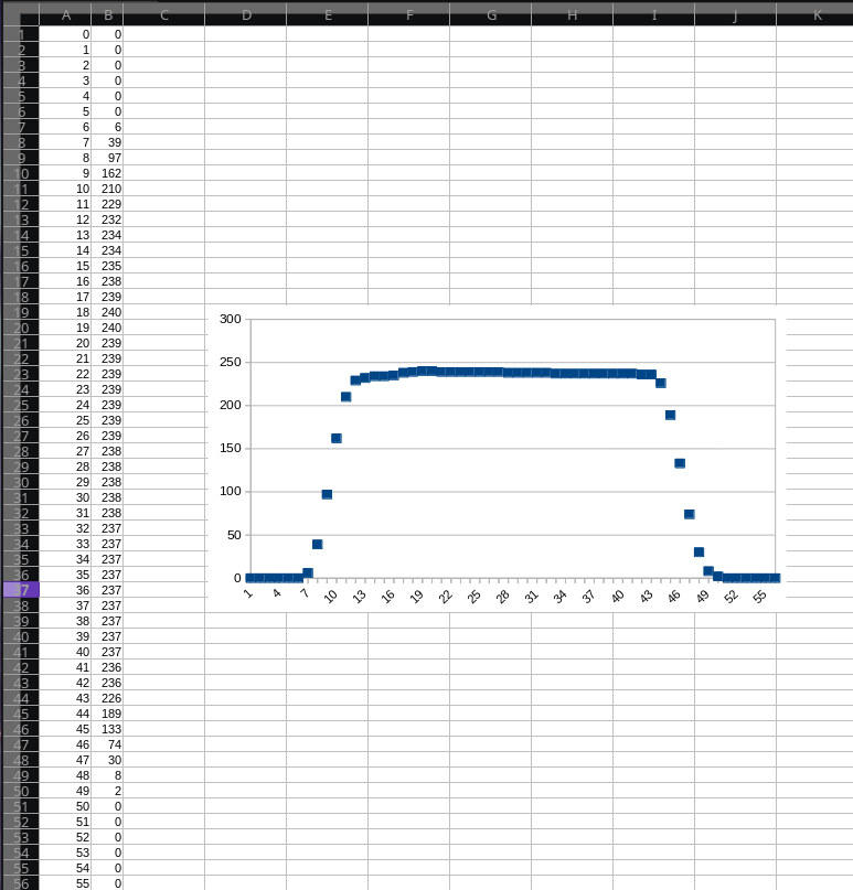
WE HAVE A PULSE! IT LIVESSSS! I was very happy to see the whole system working, but it had a long ways to go to meet the goal of this project. First of all, the front end still only supported a select few voltage ranges since the attenuators didn’t work. Secondly, the ADC’s sample rate was limited to 370 MS/s (of the 1 GS/s it was capable of) by the FT601’s maximum sustained transfer rate of 370 MB/s. And of course, software needed to be made to stream, process and display the data in real time. In my next blog post, I’ll recount how I fixed the front end issues and lowered the system’s materials cost with a new architecture!
Thanks for giving this post a read, and feel free to write a comment if anything was unclear or explained poorly, so I can edit and improve the post to make things clearer!
Discussions
Become a Hackaday.io Member
Create an account to leave a comment. Already have an account? Log In.