Schematic was inspired by various schemes from internet forums (TODO links).
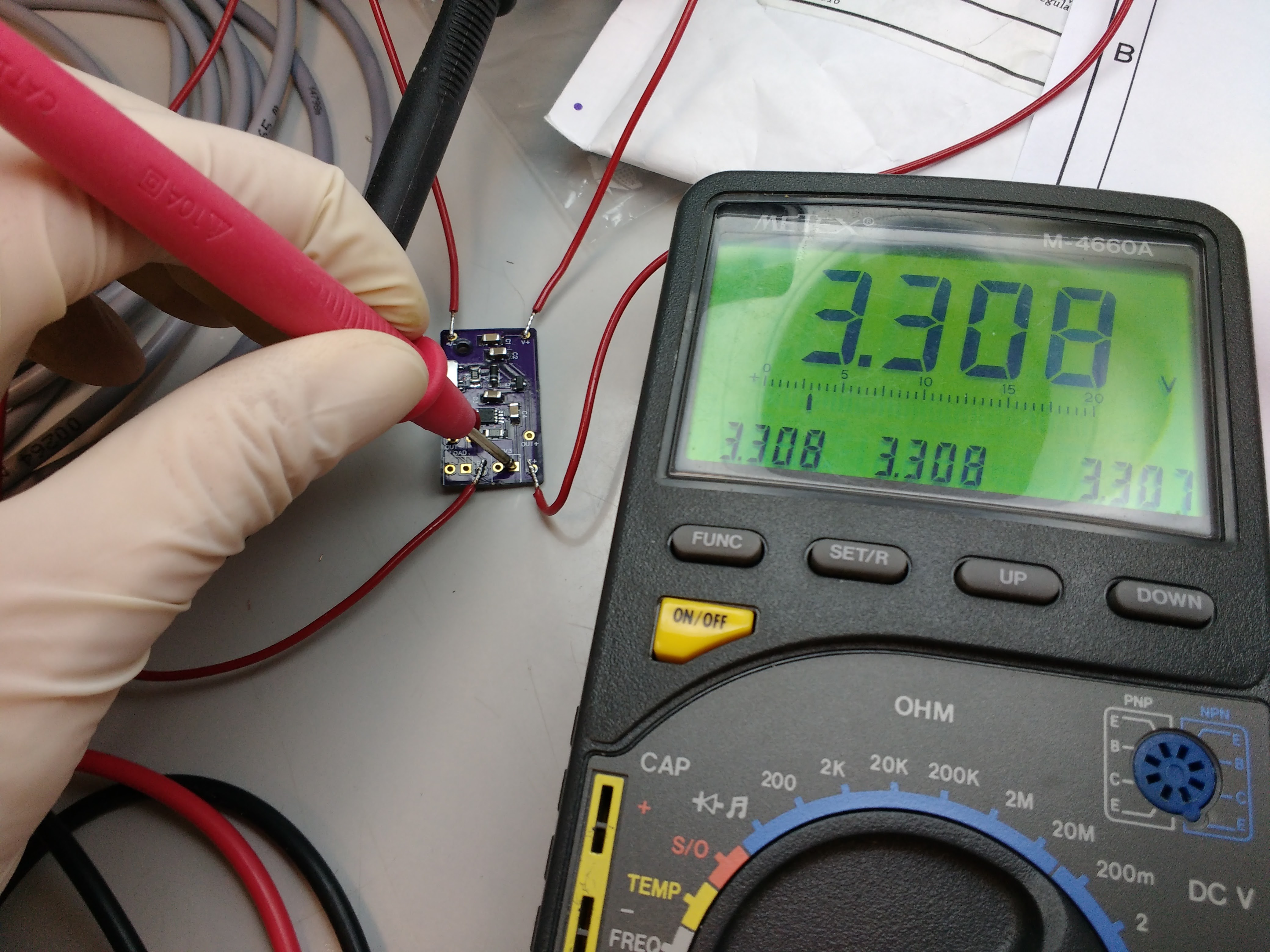
load sharing - when the Vcc is present the battery is charged and it is cut off from the load (by the Q1) while the load is powered from Vcc (via D1). When there is no Vcc the load is connected through the Q1 with the battery. Contacts LOAD are for "raw output" without the voltage regulator.
The advantage of MCP1252 is automatic buck/boost feature, it will maintain the regulated output voltage whether the input voltage is above or below the output voltage (2.1 to 5.0V input range) so it is ideal for the lithium battery voltage.
If you read the datasheet for the MCP1252-33X50I/MS there is clearly specified what type of MLCC capacitor should be used.
The PCB layout was heavily inspired by MCP1252 datasheet.
Output parameters are:
- max. output current 120 mA
- output voltage 3.3 V
There is also a MCP1253 which is identical to MCP1252 but has higher switching frequency (1MHz).
 Robert


 Bud Bennett
 James Fowkes
 Sagar 001
Thanks for the walkthrough! I'm thinking of replicating the load sharing behavior but with some other voltage regulator and had a few questions for you.
What's the purpose of adding C1 and C2? In the MCP1252 datasheet they mention C_IN for filtering noise and ripple, but aren't such capacitors included in the TP4056 board already? I can't seem to find a schematic of the board but I see a few capacitors on there, and wondered if they are already equipped or not. If they are already on the TP4056 board, then is there some other reason you found in order to motivate them being there?
Also, shouldn't the transistor be a depletion type rather than the enhancement type shown? Otherwise the transistor would be normally off and turn ON when the VCC is applied, leading to both VCC and the battery connected to load. Don't you want the battery to power the load when VCC is OFF and VCC to power the load when ON?