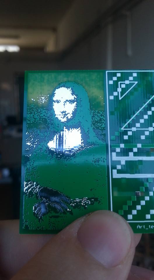
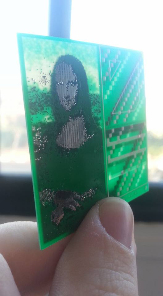
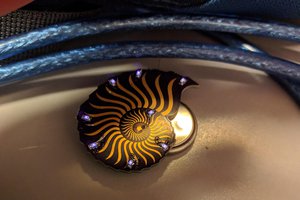
I made a tool that converts an image into multiple PCB layers - pixel brightness to board opacity. (for use with Eagle)
To make the experience fit your profile, pick a username and tell us what interests you.
We found and based on your interests.
or: How I Learned to Stop Worrying and Love the Board
Alon Gruss 20/11/16
Tl;dr:
I made a tool that converts an image into multiple PCB layers - pixel brightness to board opacity.
1. You are not limited to your discipline!
As a Designer by trade I like to jump head-first into new disciplines which I know nothing about, learn to control the terminology and try to mess around in unexpected ways. I am also lucky to share studio space with Arkadi Rafalovich, A talented engineer and omni-potentialite, who inspires and guides me through learning the basics of electronics and Eagle PCB design.
While diving into the subject I was constantly visualizing and thinking about the tools that are missing for me, the tools I need for implementing my art and design.
(I recommend Sparkfun’s tutorials).
2. Most PCB’s are boring!
PCB’s are usually designed functionally without any visual attention, A very boring rectangle. Sure, they have their digital charm with mazes of tracing running along the board, but as a user, I prefer my PCB’s when they're inside my products. Covered in a well designed injection-moulded shell.
I use the word ‘usually’ because sometimes you get boards like the Defcon badge - which can masterfully merge function and design to create a fun user experience.
Or this wonderful PCB-USB-Business card by Frank Zhao.
3. The Artist in the Engineer
So, what’s different in business cards and convention badges? These are where the engineer isn't working for a client, he relaxes a bit and has fun with the design tools. He’s not just a cog in the product development process. When he has no restrictions.
Sadly, even then, the board designer dare only to use the tools given. Drawing only in the ‘Silk’/’Copper’ layers or slightly shaping the board’s outline in the ‘Dimension’ layer.
4. All the layers!
Some of my past Design projects deal with layered/laminated materials and the smart use of the different layer properties:
Those were opaque materials. What intrigued me with PCB design-wise, was the ability to play with material’s opacity and the light transfer through the board. Artistically I thought I can convey a more complete message and user experience by having graphics that support and integrate with the board’s functionality.
5. Testing the hypothesis
I searched google for leonardo da vinci’s portrait of Mona Lisa (which I consider globally identifiable) and saved one of the results to my PC.
Opened it up in Gimp. scaled it down (nearest neighbour) and duplicated it to a couple of layers.
I then run a threshold filter on the layers changing the value a bit in each one and saved the layers to separate files.
Only then have I noticed that the new versions of Eagle already have a built-in script for importing image, from colors to layers. “That’s great! This saves me a lot of time” or so I thought.
Don’t misunderstand, It's a really great tool, just not for my purposes.
You see, I need to control the cumulative combination of layer opacities in order to achieve my goal. I aim for the PCB to be facing up (showing the top layers).
For example:
We also have:
You might have noticed that some layers control the lack of material and must be treated as a negative. That’s a bit confusing, so here is a guide table:
( legend: x = no || ⎷ = yes || ? = doesn't matter || n = inverted ) |
Color (layer No.) | Top (1) | Bottom (16) | tStop (29) | bStop (23) | tPlace (21) | bPlace (22) |
0 | x | x | ⎷n | ⎷n | x | x |
1 | x | x | x | ⎷n | x | x |
2 | ⎷ | ? | x | ? | x | ? |
3 | x | x | x | x | x | x |
4 | x | x | x | x | x | ⎷ |
5 | x | ⎷ | x | x | x | x |
6 | x | ? | x | ? | ⎷ | ? |
7 | ⎷ | ? | ⎷ | ? | x | ? |
6. Lessons learned
I ordered the boards from Seeed...
Read more »
Create an account to leave a comment. Already have an account? Log In.
Thanks, I'll check it out!
Neon22- I'm aiming for a standalone app, in "java", that converts raster images to layers in Eagle .brd files. So you can see how an Inkscape extension in python is a bit out of my scope at the moment. I am however planning to integrate .svg vector files.
yeah - it would be really great if you coudl add an inkscape extension (python mostly) that did this and integrated it with Saar's work... Happy to help out with inkscape extensions - I've made a few
Become a member to follow this project and never miss any updates
About Us Contact Hackaday.io Give Feedback Terms of Use Privacy Policy Hackaday API Do not sell or share my personal information
Check out PCBmodE.
It's basically a tool that allows you to jump back and forth between a rudimentary script and Inkscape, and then finally exporting the gerbers. Many of the boards created in it are exactly what you're talking about - art pieces first, and possibly functioning PCBs second.