EtchedPixels
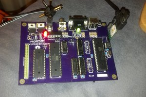
Although the hardware supports both a Motorola and an Intel style bus we actually use the Motorola interface. This is because the RTC expects a multiplexed Intel style bus as used by the 8085 and some microcontrollers. It's actually easier to abuse the Motorola bus interface and wire it to a pair of I/O ports. This is the same trick used on a lot of different existing systems.
U2 generates a low for a suitable address space match. That is used to drive the chip select and also combined with A0 so that a write to the low address causes a pulse on AS making the chip latch what it thinks is a multiplexed address and also with \A0 in order to generate a second pulse on DS, which it thinks is the data half of the multiplexed address. RW is driven from the bus write line. Although this isn't a Motorola RW line it always has the right value we need whenever the chip is selected.
JP1 allows the square wave output to be coupled to a user bus line. JP2 is the goodl old 'clear NVRAM' jumper.
 Samuel A. Falvo II
 Keith
Keith
 Jac Goudsmit