 ElectroBoy
Last week, I designed a Bluetooth PCB for my homemade home theater and amplifier system. And these are working fine with circuit. You can see our last design from here, but now I want to upgrade it. I want to make a PCB for my car amplifier system as a USB input.

As you know I am using JL-series Bluetooth IC and they support the USB (D+ and D-) feature. So, I tried to go with the same. Here is some info and specs of the Bluetooth receiver IC.
JL series Bluetooth chips (AC6939B_SOP16):
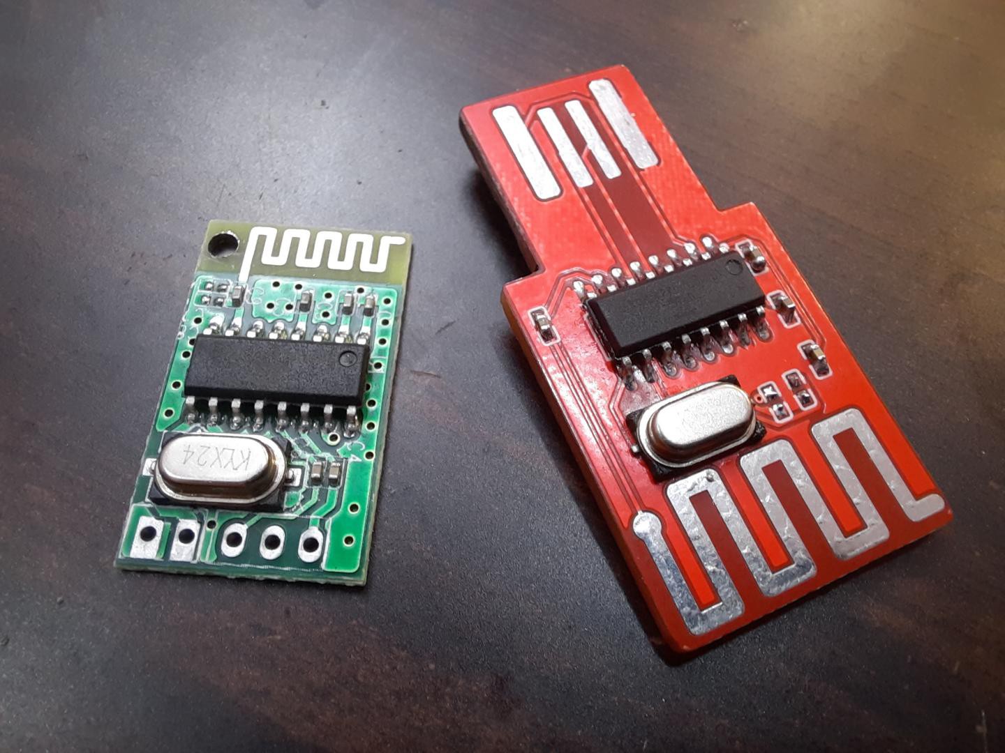
Nowadays, these are very popular, highly integrated and cheapest ICs with a lot of features. Available globally and manufactured in China, yet there is no any details or datasheets about them on web. I think manufacturer doesn’t want to disclose the info.
How I got Pinout and circuit:
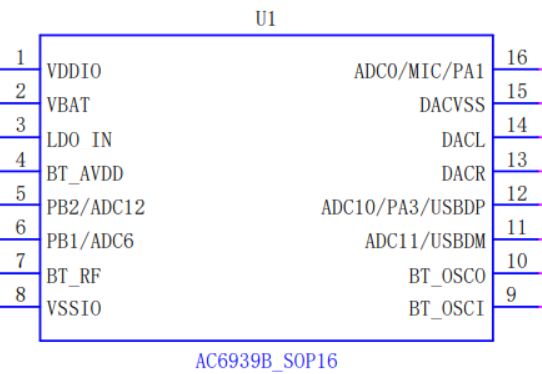
After searching the specific IC number with package details, SOP 16 pin. I found a website chenbingdom.com, that may give the pin details and circuit description about this JL series ICs. This website uses a http: unsecure connection, so make sure before you reach to them. All the PDF and datasheets are in Chinese language and provide only the schematics of the circuit. Which can be modified further as per requirements.
Features of my version chip (AC6939B_SOP16):
1) Frequency range: 2402-2480 MHz
2) Modulation type: GFSK (Battery life saving technique)
3) Working voltage: 3.0 - 5.5volts
4) Low power consumption: 14mA @4volts
5) Low components used
6) Clock: 24 MHz Crystal
7) Stereo mode available
8) USB supported
9) Onboard Mic options
10) Led indicator mode available
11) AD Key supported (Increase/ Decrease volume and channels)
12) 10-meter range
Circuit Diagram:
This is circuit for chip 6939B, you can get specific IC pinout and schematics from Here.
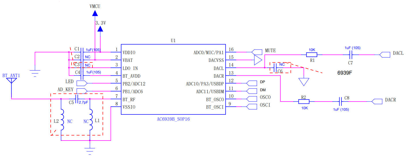
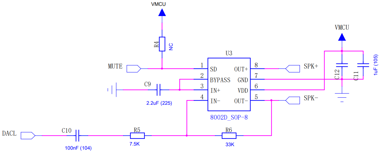
In the circuit 24MHz crystal oscillator is used without capacitors in series with it. Also, the SMD inductor is not mandatory to use. This ic supports dual channel audio out, so we can use this with stereo audio amplifier systems.
Modified circuit layout:
The real operating circuit do not need too many components, that's why I draw a simplified schematics by my own.

Just ignore the IC pins and name. I am using ch340g in the schematics because this bluetooth IC is anonymous and package is same SOP16. You can see the Real pinout in above image from this. In case you want to modify anything you can download the Gerbers from here. If you want to use my layouts then open source link is here.
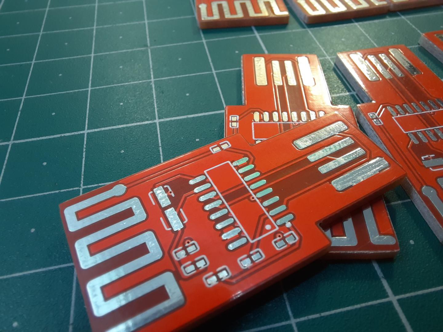
PCB Layout:

After making a cool circuit, I designed the PCB in Easyeda and Order it from JLCPCB. They are offering the PCB prototypes in cheapest. I got 30pcs of these small PCB with the thickness of 1.2mm and red color Hasl finishing just in $5. Download Gerber files from here.
And here is a special offer for you guys, Sign-up to JLCPCB using this link and get free coupons worth $27. Try their SMT assembly service to get rid of soldering and assembly process.
The ordering process is also quite simple, just follow these steps.

Go to JLCPCB> Upload Gerbers > Select quantity, color and surface finish> Add to cart > Checkout and receive package within 7 days.
Components Required:
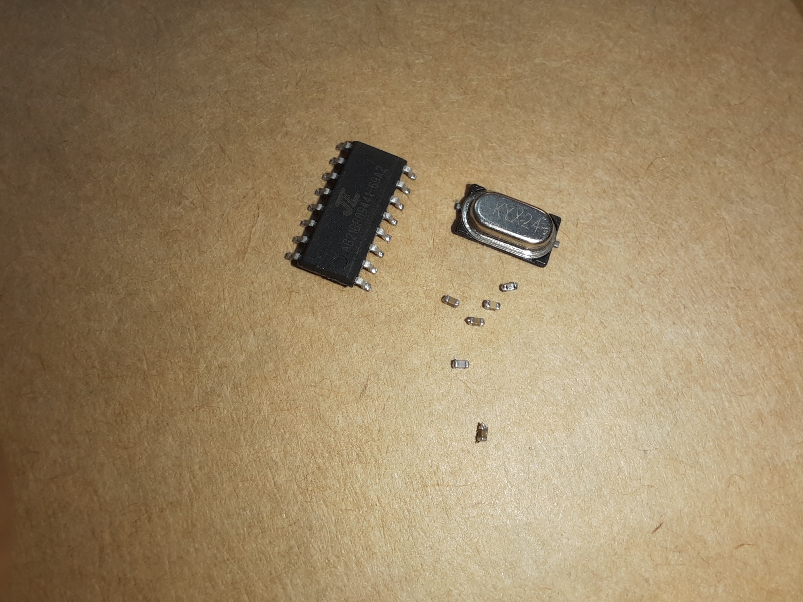
1) AC6939B_16_SOP Bluetooth Ic
2) 24Mhz crystal
3) 100nf capacitor
4) Wires and connector
5) 5v battery
Soldering And Assembling:

I opened the PCB packet and choose one piece for first try. Then I gathered all the components and print the circuit diagram on a paper for assembly.

We can solder all the components using hand soldering method and I think this is the best one for now instead of any costly hot plate.
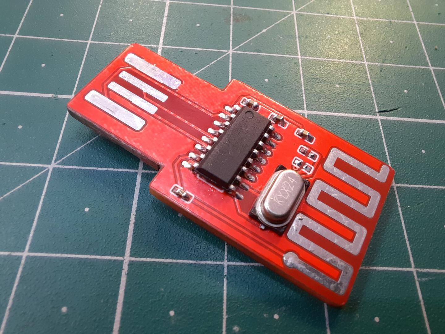
After soldering clean the pcb with petrol or alcohol to remove residual flux.
PCB Form factor:
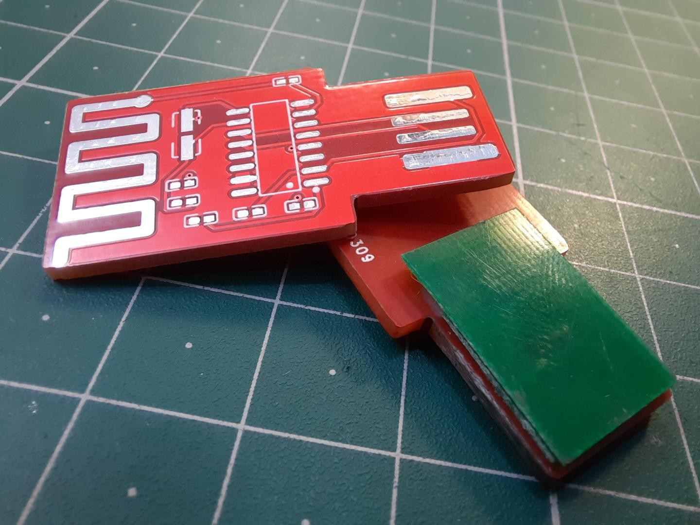
Because My pcb is of 1.2mm so I glued two spacers behind the USB, this will help to make good connection and fill the gap between the PCB and USB (female type).
Connecting with mobile
As you know these are 3.0 version of bluetooth IC's and named as 3.0 by default in the flash section.

Just plug the USB and...
Read more »
 Chris
Chris 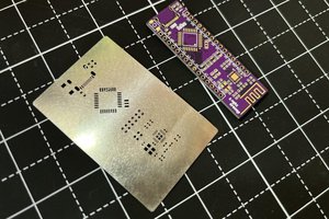
 Sagar 001
 mbsg99