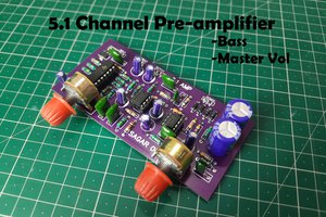
I made many amplifiers and preamplifier project in past. But due to the continuous demand I have some new Ideas about amplifiers. But all of them are half without a proper preamplifier circuit. Because preamplifier not only boost the signal but also arrange low and high pass signal on different output channels. Looking into the concept of 4 channel surround sound system, I want to design a 4-channel audio output buffer with adjustable volume control function.
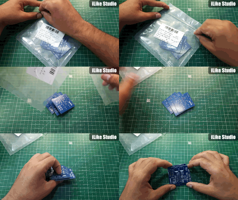
This type of buffer circuit takes 2 channels as input and give 4 channels of output. Each output can be further modified as per frequency adjustments for speakers, subwoofers and twitters. Because there are a lot of connections and I want to make best in 1st attempt, I choose JLCPCB PCB prototype service to get my hands on best PCBs. JLCPCB is one of the leading companies and very reliable solution for prototyping providing 5pcs of 2layer PCB in just $2.
LM324:
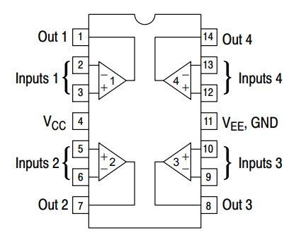
These devices consist of four independent, high-gain, frequency-compensated, operational amplifiers that are designed specifically to operate from a single supply or split supply over a wide range of voltages. Because of these 4 built in OP-amps, we can get 4 channel output of the supplied signal with adjustable gain.
Features:
Wide supply range: 3 V to 30 V
· Low input offset voltage maximum at 25°C: 3 mV
· Low input bias current maximum at 25°C: 35 nA
· 2-kV ESD protection
· Internal RF and EMI filter
· Low quiescent current of 175-µA/ch typical
· Common-mode input voltage range includes VCC–
· Differential input voltage range equal to maximum-rated supply voltage
· Open-loop differential voltage amplification: 100-V/mV typical
Why we need Op amp for preamplifier:
Operational amplifiers are the basically used to increase gain of the signal. By changing resistor values we can change the overall gain and peak voltage.
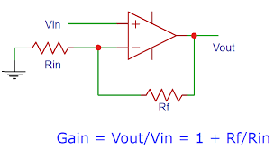
As shown in the figure, the gain value is depended on Rin and Rf. Gain of this non-inverting operational amplifier is further given by:
GAIN= Vout/Vin = 1+Rf/Rin
In our circuit, we increased the gain by a factor of three. Here Rf is 22k and Rin is 10k. The circuit with no gain means without any resistance is known as voltage follower configuration.
Gain: 1+Rf/Rin= 1+22/10 = 3.2
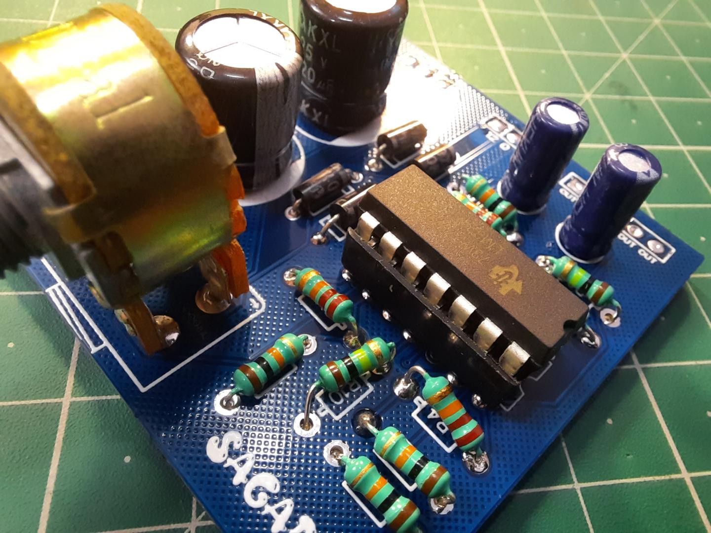
If you want to increase the gain more, then change the values of these resistor or replace one of them with same value potentiometer. But further increase in gain may produce noise in the signal.
Components required:
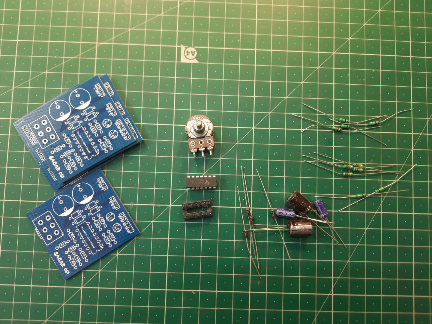
1) LM324 operational amplifier
2) Custom made PCB from JLCPCB
3) 22k, 10k and 100k resistors
4) 100k potentiometer
5) 1N4007 Diode
6) 2200uf, 2.7uf Electrolytic capacitor
7) Pin headers
Circuit diagram:
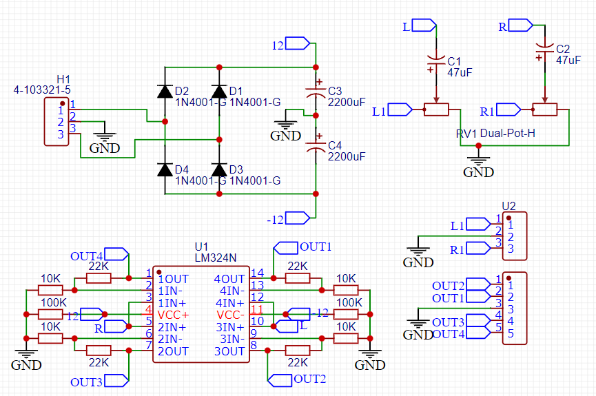
LM324 has 4 channel Operational amplifier, we need to repeat the configuration of resistors with each so that it can give 4 channel output. I choose 3.2gain for this buffer circuit and a 100k potentiometer for master volume control. 10k, 22k resistors are Rin and Rf respectively, 100k resistor is to give proper biasing to the operational amplifier.
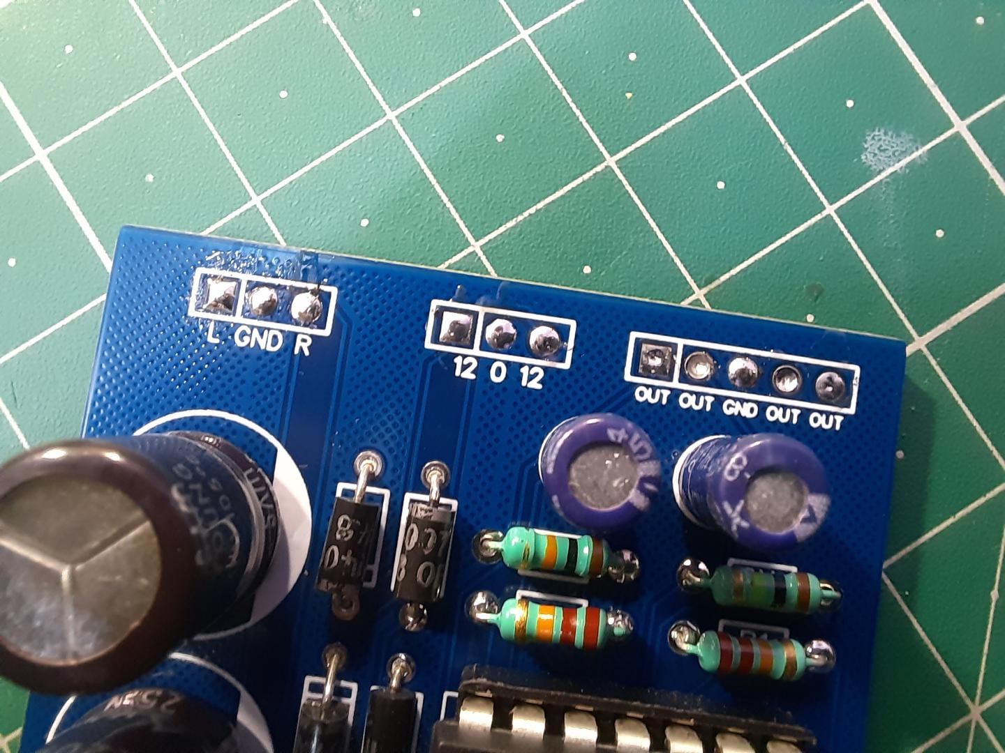
Two small value electrolytic capacitors are used in the circuit as coupling capacitors(Blocks Dc to flow). Because my circuit works on dual voltage, I made an onboard power rectifier section with filter. All the connections are given through male pin headers.
PCB layouts:
If you want to keep continue with my designs you can download the Gerber files and circuit diagram from here.
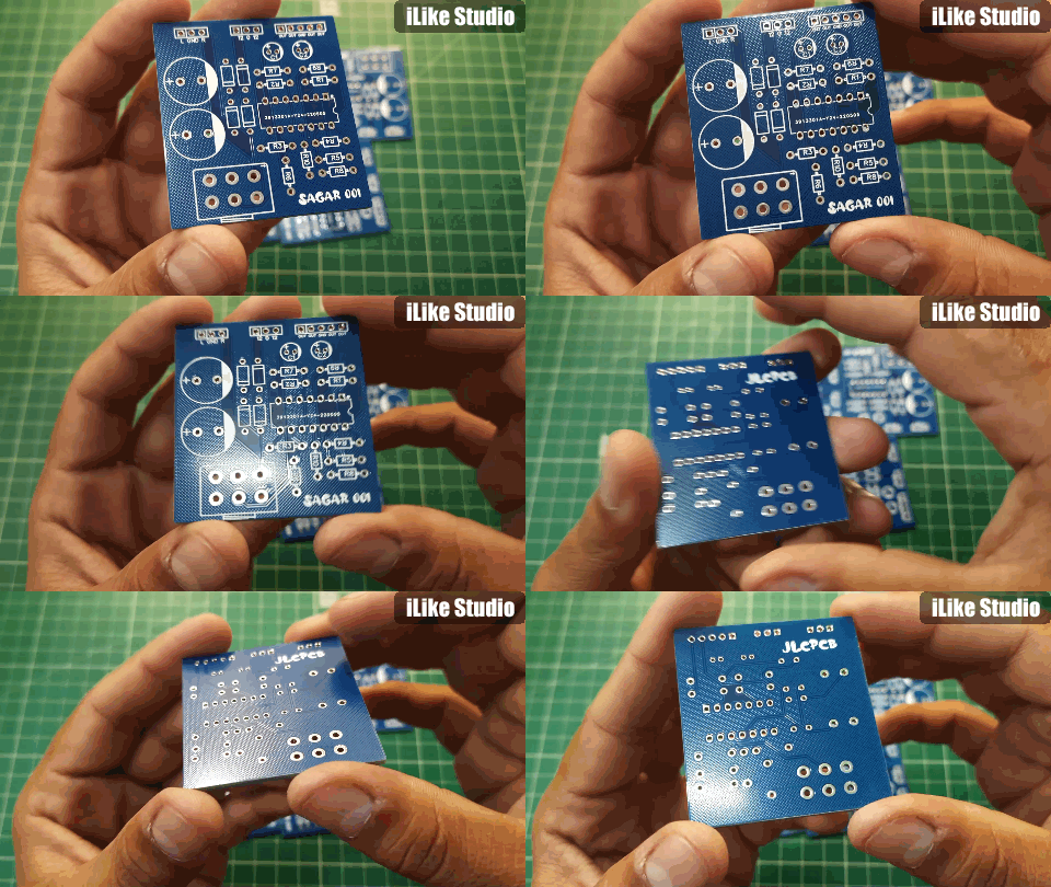
I choose blue colour, Hasl finish, 1.6mm and FR4 material for my project. To order the same PCB, Go to JLCPCB and upload your Gerber files. Choose all the parameters and add your pcb into cart.
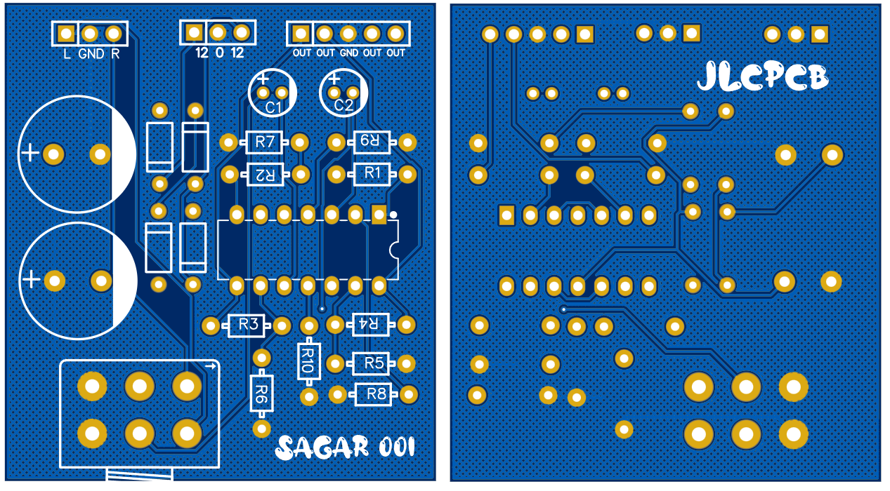
You will get your designs in just 7 days after dispatching. And if you sign-up using this link you will get free coupons of $30. Checkout to JLCPCB right now and get hands on best PCBs ever.
Connections:
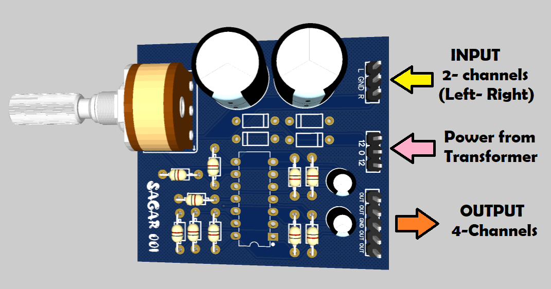
Supply this board with a center tapped transformer with 12-0-12volts @500mA. Input is supplied with...
Read more » ElectroBoy
 Sagar 001
 Ghani Lawal