 h2w
h2wThe Concept
The concept of the project was based on the idea of a new version of Amstrad CPC6128 computer - using modern components and up-to-date technology. Subsequently, this concept underwent a number of significant changes. One of these changes was the idea to equip this clone with Aleste extensions.
For reference: Aleste 520EX (A520) - is a Russian clone of Amstrad CPC6128 computer, but with some extensions. The main advantage of this computer was its sound capabilities, which were comparable with Amiga 500. The Aleste computer could play 4-channel mod files - it had a sampler synthesizer. Among the disadvantages were the high complexity of the assembly, as well as the very rare components today. Another drawback was that the A520 had two completely incompatible Aleste and CPC modes. That is all cool features of A520 were not available for CPC programs. This was the flaw that I needed to fix first.
Re-reading the book may surprise you with interesting details. But your new interpretations can be even more interesting and dramatically different from previous ones. Along the way, the project changed and its final formula for the new computer, which is called XiAleste, became the following:
- XiAleste is primarily an Amstrad CPC with extensions available to it from the A520.
- The A520 extensions will be redesigned -- the spirit of the A520 will remain.
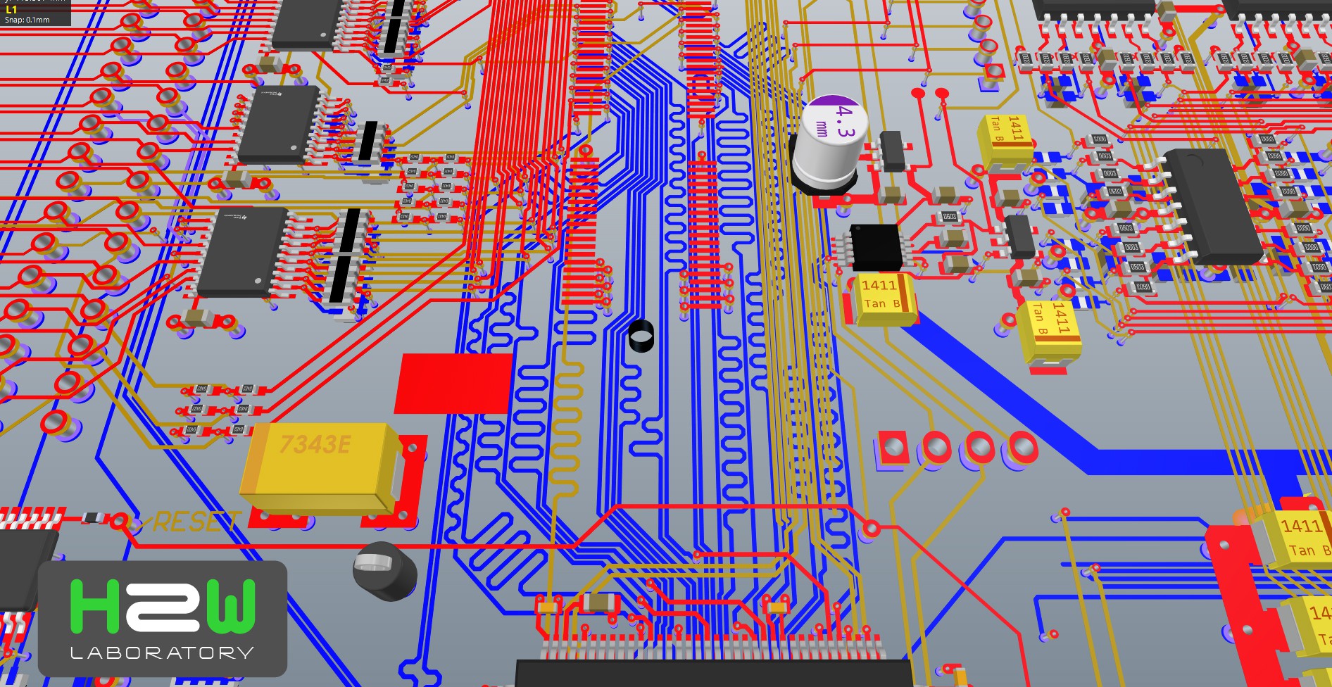
- XiAleste is 100% open source. All source files of the project will be published on github.
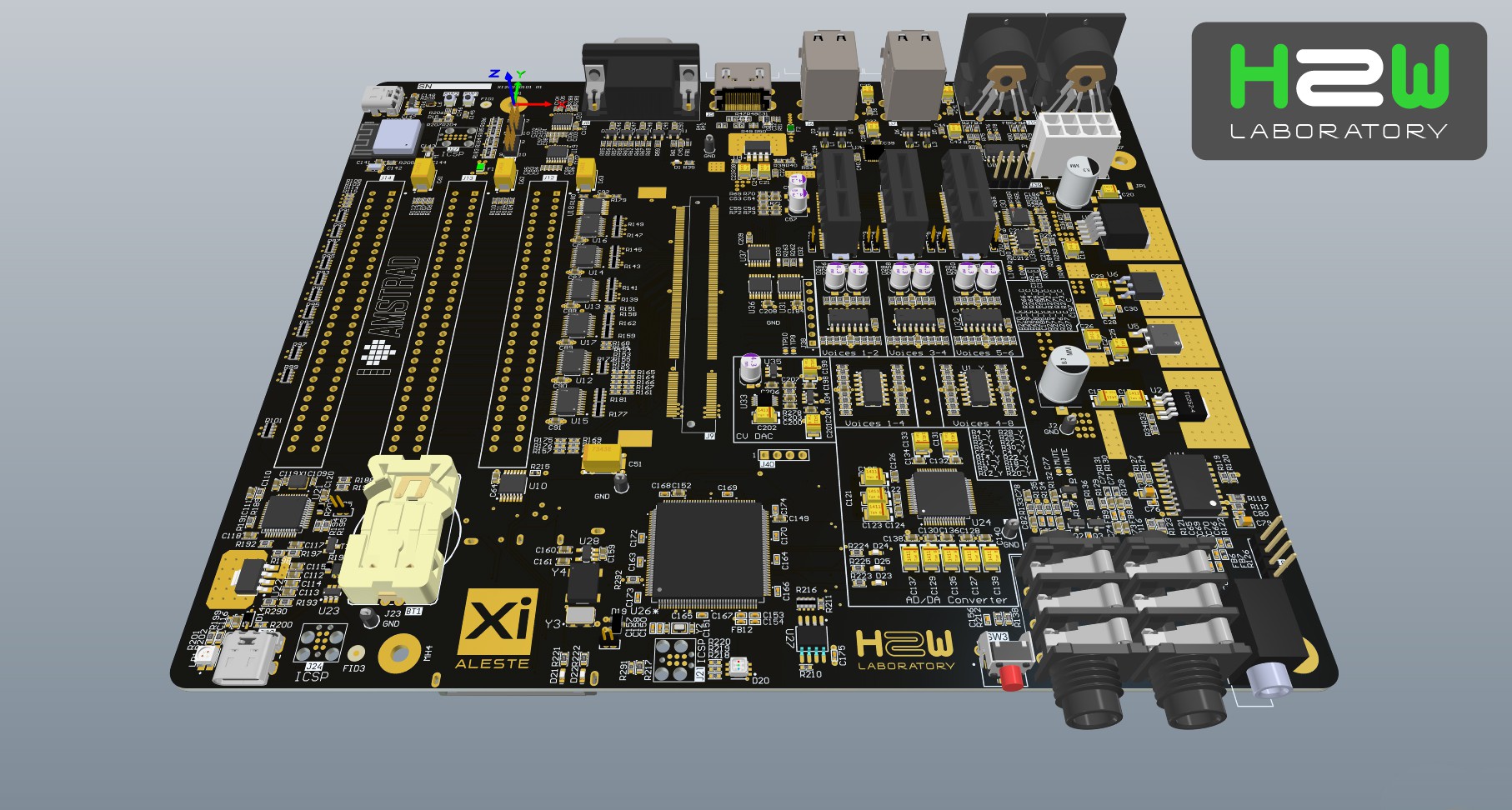
The XiAleste computer is a sound synthesis platform which cannot be fully emulated on an FPGA, i.e. a MIST or MISTER type board. This computer will have its own unique architecture. This architecture will have:
- A bus for extension boards -- primary for digital peripherals devices.
- A basic sound synthesizer system that can be extended.
- Bus for sound extensions -- analog sound processing modules.
The project is very ambitious and I can not give a 100% guarantee for its quick and complete completion. But if there are people who want to get involved and help, chances are better.
The Spirit of Aleste
This is a retro computer project, so all changes must be made with great love and respect for the engineers who created the amazing Amsrad CPC6128 computer.
One of the major extensions of the Aleste is the MagicSound sound card. You could say it is the cornerstone of the project. Having a board of this class requires many more signals on the extension connector - more than on the CPC6128 connector. These signals are used for direct access to the memory located on the motherboard. It is important to note that the ability to access the entire address space of the computer at will is another distinguishing feature of the A520. Although it is not necessary if the sound system is located on the processor board. Nevertheless, the improved expansion slot is something valuable to realize.
Precisely because this connector is not known to be CPC6128 compliant it can be radically modified. There are also no plans for compatibility with the A520.
Amstrad Expansion Bus
I chose the ITX (DTX) standard as the printed circuit board design. Along the way I noticed that the original Amstrad CPC6128 connector can only be placed on the right side of the PCB. So, unfortunately, I have to give it up. But you can modify the board design and return it to the system.
XiAleste Expansion Bus
The Amstrad CPC6128 connector can be classified as a Processor Direct Connector (PDC), and the Aleste expansion connector can also be classified as such. I plan to evolve this connector to an 8-bit parallel computer bus and install two or three sockets on the board. The Amstrad CPC6128 connector for hardware compatibility can be put on the board as the same PDC without any changes.
Memory Map
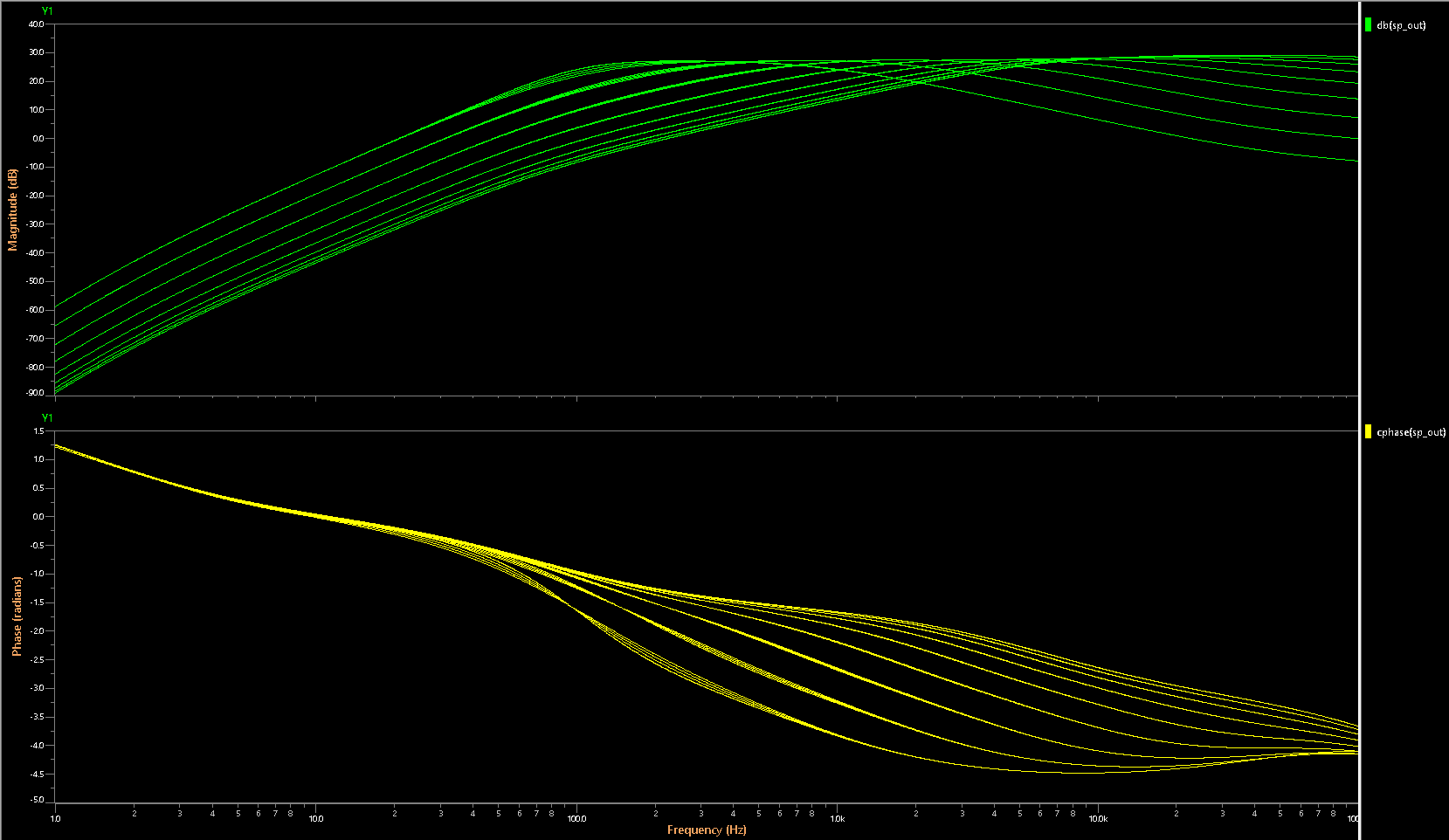
Another important feature of Aleste is the use of MSX Mapper as a memory manager. However, this has been done with certain limitations. The fact is that the highest two bits of data in the Gate Array...
Read more »

 Neven Boyanov
 Kn/vD
Kn/vD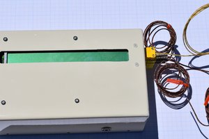
 Bharbour
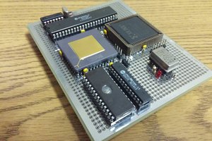
 Jason Westervelt
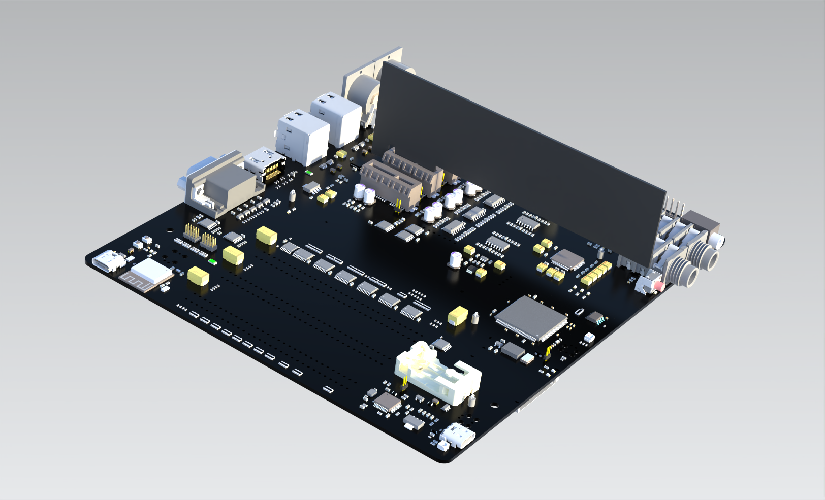
In principle, this is interesting because KiCad makes the project more friendly to the OpenSource community. But it is embarrassing that this board has not been produced and tested, which creates a feeling of prematureness. Nevertheless, I suggest you decide for yourself.
With great respect,
h2w