Sungwoo
Overview of FPGA modules
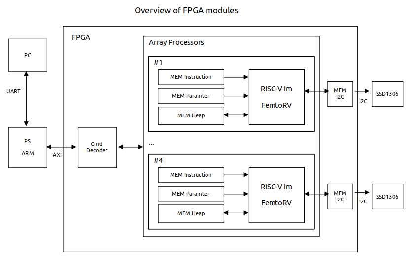
First, kudos to the FemtoRV project (https://github.com/BrunoLevy/learn-fpga). Each extension of processor ( electron used here ) is a single Verilog file and it can easily added to your project, and it works flawlessly.
This project adds input/output capabilities, memory, I2C, an interface to the host, Verilog verification, Xilinx Vivado support, compiler support, CMake, and a GitLab pipeline.
I burned the code to the Zynq (Minized) platform, so all of the hardware descriptions are based on that platform. Well, I know, that Minized is already obsolete, but this work should be applicable to other Xilinx Zynq platform easily.
All of the memory is BlockRAM on the FPGA, and it is very small. Each instruction memory is 4kB, parameter memory is 4kB, and heap memory is 4kB. You can increase the memory size in units of 4kB, as each BlockRAM is 36kbits. This means that you can have a maximum of 1k instructions. However, if you need more, you can increase the size as long as it does not exceed the total BlockRAM size of 50.
The memory can be initialized with predefined values. A data file can be used to store 32-bit hexadecimal values, so that the memory can store instructions to be executed as soon as the processor starts, just like a ROM. Alternatively, you can upload instructions with the provided Python script and execute them, just like a RAM.
Parameter memory is used to store processor-specific information, such as the processor number. It can also be initialized with a data file or uploaded at runtime.
Heap memory is used to store temporary variables and the stack, so that C++ code can run just like it does on a normal PC. However, there is no support for 'new' or 'delete'. For debugging purposes, the heap memory is cloned so that the user can peek into it to see what is going on inside.
To control 128x64 display - SSD1306, mem i2c module is connected to the processor so that it can write a value on a IO memory region and it will drive the i2c bus.
 f4hdk
f4hdk
 Erik Piehl
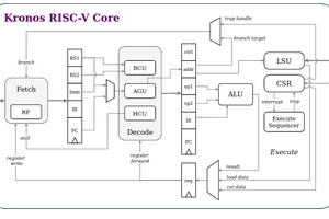
 Sonal Pinto