Introduction
In the past, I have undertaken projects involving portable oscilloscopes with high-speed ADCs (as seen in RPScope). However, in this endeavor, I am committed to streamlining the electronics to the utmost extent and utilizing only the capabilities inherent in the STM32 platform.
The STM32G4 family features a multitude of analog peripherals that prove instrumental in minimizing the Bill of Materials (BOM), encompassing 4 ADCs, 2 DACs, integrated OPAMPs, and more. The only external used parts are two OPAMP ICs mainly to protect the MCU from overvoltages from input channels. The power supply aspect has also undergone simplification; departing from the conventional symmetric power supply configuration often employed in such projects, I have exclusively employed a single-ended power supply, further enhancing electronic simplicity. Despite this departure, it remains possible to capture negative voltages by introducing an offset at the input stage.
The oscilloscope boasts a 480x320 resolution display, from BuyDisplay, interfaced via a 16-bit bus and mapped to the STM32's memory, affording rapid data transfer and achieving an impressive frame rate exceeding 50 FPS, though tactically limited to 20 FPS to ensure CPU availability for other concurrent tasks. The graphical user interface is materialized through the port of Nuklear libraries – originally intended for PC gaming – written in ANSI-C, with a modular design, and seamlessly executable within the microcontroller's.
The hardware fabrication was entrusted to JLCPCB, a 4 layer PCB following their stipulated minium design constraints of 0.1mm trace separation and width, along with 0.35mm via diameter. While not strictly necessary for this design, I was intrigued to assess the outcomes, which proved impeccable. A touch of Artificial Intelligence was also interwoven into the project (Midjourney), albeit indirectly, manifesting in the incorporation of "Mechwarrior" robot drawings within the PCB silkscreen layer, imparting a distinctive visual flair.
With regard to software, my original intent was to integrate MicroPython, an ambition that prompted a Nuklear port to the MicroPython ecosystem. However, due to constrained RAM resources, I have chosen to forge ahead in the development process using the C programming language, complemented by the FreeRTOS operating system framework.
Hardware
The hardware design is characterized by its simplicity, primarily comprising the STM32 microcontroller, two operational amplifiers (OPAMPs), a battery charger, and a TFT display.
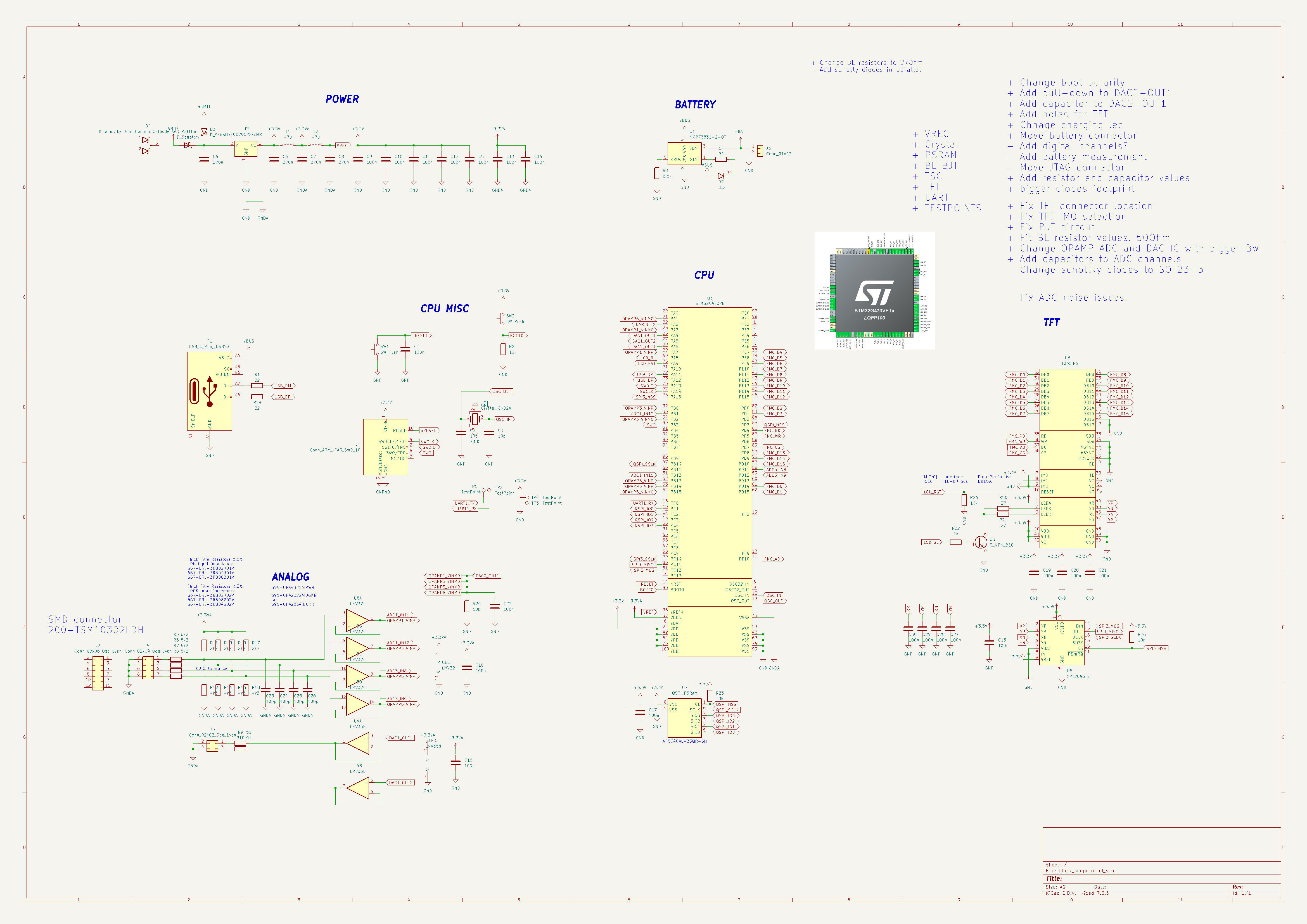
Power
The power subsystem revolves around a 3.3V regulator and a LiPo battery charging module. With the USB connection established, the entire system is powered via USB while simultaneously charging the LiPo battery. When USB power is absent, current is channeled to the voltage regulator through a Schottky diode.
The analog voltage is derived directly from the digital realm and is subject to minimal filtration through inductors. Although the prospect of integrating a dedicated regulator has been contemplated, current circumstances have not warranted its implementation. An intrinsic advantage of this design lies in its obviation of the need for symmetric power supply, significantly streamlining the Bill of Materials (BOM).
In this iteration, the analog and digital ground planes are interconnected, rendering the presence of separate ground planes unnecessary. Subsequent iterations will explore designs featuring isolated ground planes to assess their impact on noise mitigation, particularly when measuring low-amplitude voltages.

The battery charging module is embodied by a straightforward SOT23-6 IC, proficiently facilitating the charging of a 130mAh LiPo battery. An LED indicator illuminates during the charging process, extinguishing upon completion. The charging cycle is approximately one hour, affording an operational span of roughly two hours. While this duration may seem limited, deliberate consideration has led to the selection of a compact battery footprint, with the understanding that the oscilloscope can readily interface with a power bank when extended usage is requisite.

The battery supplies around 3.7V, while the circuit's operational consumption hovers around 80 mA. Notably, the voltage drop of Schottky diodes, measuring approximately 400mV at this current level, imposes a slight constraint on the voltage arriving at the voltage regulator. Accordingly, future enhancements contemplate the parallel integration of two Schottky diodes, thereby mitigating the per-diode current load and subsequently reducing the voltage drop.
CPU
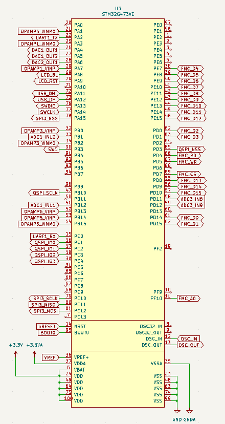
At the heart of the system lies the STM32G474VE, a Cortex-M4F processor operating at a clock frequency of 170 MHz. This microcontroller, housed within a TQFP-100 package, boasts a commendable 512 KB of FLASH memory and 128 KB of RAM. As it stands, the codebase occupies a modest 20% of the available FLASH memory, while the operational demands consume 90% of the allocated RAM. Furthermore, the hardware interface consumes half of the available GPIO pins, attesting to the judicious resource allocation.
The extensive repertoire of integrated peripherals inherent to this microcontroller has been a pivotal enabler in substantially curtailing the Bill of Materials (BOM). In particular, the inclusion of 4 ADCs has been instrumental. Equally noteworthy are the integrated Operational Amplifiers (OPAMPs), which, beyond their conventional utility, serve as Programmable Gain Amplifiers (PGAs) with independent offset inputs. This versatility considerably enhances the system's functionality, providing an expedient means to accommodate varying input conditions.

TFT and TSC
The TFT display boasts an impressive resolution of 480x320 pixels and is underpinned by an ILI9488 controller. Its seamless linkage to the CPU is facilitated through a 16-bit 8080 parallel bus, establishing a robust connection to accommodate high-speed data transfer.
Leveraging the Flexible Memory Controller (FMC) peripheral, the CPU leverages a memory-mapped approach to interface with the LCD. This expedient method of data access not only expedites image rendering but also contributes to achieving a remarkably elevated frame rate, surpassing 50 FPS. The FMC's capability to treat the LCD as a seamless extension of memory significantly enhances data transfer efficiency.
The procurement of TFT displays extends beyond the mere acquisition of integrated components from established suppliers like Mouser. Often, the pursuit of cost-effective solutions on platforms like Amazon or AliExpress leads to encounters with inexpensively priced displays lacking comprehensive documentation – including datasheets, pinouts, and dimensional specifications. A reliable resource that addresses this challenge is buydisplay.com, offering a wide array of displays accompanied by the requisite documentation, thereby streamlining the integration process.
The Touch Screen Controller (TSC), linked to the CPU through an SPI bus, operates proficiently at a 1 MHz read rate. Throughout the software development phase, it became evident that the TSC measurements exhibited a certain level of noise, prompting an increment in the reading frequency to enable effective filtering. Initial attempts to mitigate this noise by introducing capacitors to the XP/XN/YP/YN lines, as manifested in the schematic design, yielded inconclusive results upon evaluation. This aspect remains a focal point for further investigation, as the endeavor to optimize noise reduction continues to drive ongoing exploration and refinement.

Two areas for improvement within the design warrant attention. Firstly, the integration of an IPS (In-Plane Switching) TFT display, renowned for its superior visual quality and notably enhanced viewing angles. Although these displays are readily accessible through sources such as buydisplay.com, an unfortunate oversight in the procurement process led to the selection of an alternative display technology. This adjustment promises to significantly elevate the overall user experience, culminating in enhanced visual fidelity and broader viewing perspectives.
Another imperative aspect pertains to luminosity considerations. The interplay between luminosity and battery life, dictated by the constraints of a compact battery, assumes prominence. Elevated luminosity invariably exerts a commensurate impact on operational endurance. Consequently, to ensure a duration exceeding one hour of usage, luminosity was consciously minimized. Balancing luminosity against battery longevity becomes a pivotal endeavor, necessitating strategic optimization to attain an equilibrium that extends operational span without compromising display visibility.
Analog Input and Output Stage
The input stage comprises five distinct blocks, with some of them integrated within the STM32:
-Resistor Divider and low pass filter:
The entry point entails a resistor divider network accompanied by a capacitor for each channel. This composite configuration serves a multifaceted role encompassing impedance matching, voltage range conditioning, offset provisioning for accommodating negative voltages, and high-frequency filtration. This amalgam ensures a refined input signal for subsequent processing.
-External Operational Amplifier (OPAMP):
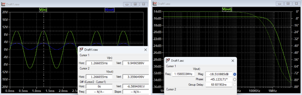
A pivotal element in the signal path is an external operational amplifier (OPAMP). Through the incorporation of the OPA4322 by TI, the signal undergoes an essential transition, functioning as an emitter follower. With a bandwidth of 20 MHz, surpassing that of the input stage, this OPAMP facilitates high slew rate signal processing without introducing distortion.
-Internal OPAMP & PGA:
Following the external amplification, the signal proceeds to the integrated OPAMP and Programmable Gain Amplifier (PGA) units. These versatile components bestow the capability to amplify the signal within a range spanning from x2 to x64. This amplification range engenders dynamic versatility, allowing the capture of signals across a spectrum spanning from millivolts to volts without necessitating external circuitry. The incorporation of an external offset input for the PGAs, complemented by the use of an additional STM32 DAC, obviates the amplification of any residual offset.
-Offset DAC:
In response to the offset introduced during the previous stages, a dedicated Digital-to-Analog Converter (DAC) on the STM32 counteracts this effect, ensuring signal fidelity and mitigating offset distortions.
-ADC:
The culminating phase entails the transmission of the amplified and offset-corrected signal to individual Analog-to-Digital Converters (ADCs), each serving an individual channel. This meticulous allocation facilitates maximum attainable sample rates for each channel, preserving signal integrity.

A primary limitation within this design pertains to the uniform offset across all channels. High tolerance in the input stage resistances could potentially encumber the amplification process of each PGA. To mitigate this, the input stage resistances were meticulously selected with a precision of 0.5%, ensuring uniform amplification performance.
Moreover, an unexpected challenge emerged involving the pins designated for PGA offsets, which concurrently serve as UART2 pins during ST's bootloader operation. Rectification was achieved through the introduction of pull-down resistors and capacitors, fostering stable DAC voltage during normal operational phases.
Transitioning to the output stage, this arrangement amalgamates the STM32's DAC, an operational amplifier, and a 50 Ohm resistor. This synergy enables the generation of diverse waveforms, encompassing PWM, sine, triangular, or even arbitration patterns, up to a maximum frequency of 1 MHz, albeit consistently confined within the 0 to 3.3V voltage range.
Furthermore, the input electronics blueprint is conceived to furnish four input channels along with the potential for two differential channels. While yet unverified, the hardware's foundational structure accommodates this prospective expansion.
PSRAM
The incorporation of PSRAM introduces a captivating dimension to microcontroller designs, notably underscored by their prevalent utilization in platforms such as the ESP32. This distinctive hardware resource unlocks the potential to harness several megabytes of memory while exerting minimal pin count and without imparting unwarranted software complexity. In this context, a PSRAM module of 8 megabytes was seamlessly integrated, interconnected via Quad Serial Peripheral Interface (QSPI), which, when synergized with the Direct Memory Access (DMA) capability, affords an impressive read and write speed of 10 megabytes per second.
This pragmatic integration delivers a manifold of benefits, including the augmentation of available memory, a cornerstone that underpins multifaceted applications. While the PSRAM does facilitate memory mapping, this functionality is tailored exclusively for read operations. As a result, the design judiciously retains access through QSPI registers, orchestrated in harmony with the DMA, optimizing data flow and enhancing overall performance.
The strategic deployment of PSRAM amplifies the design's data-handling prowess, enabling seamless data storage, retrieval, and processing, thereby bolstering the microcontroller's efficacy in demanding computational and data-intensive scenarios. This augmentation harmonizes with the ethos of efficiency and resource optimization that underpins the entire design endeavor.

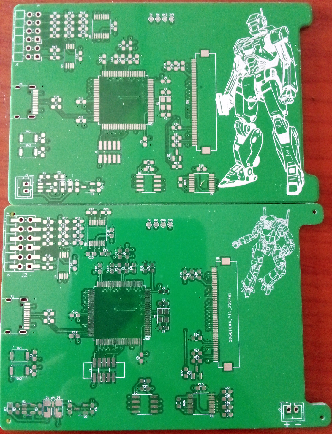
PCB
The PCB encompasses a compact form factor, encompassing dimensions of 90x60mm, carefully designed to harmonize with TFT display specifications. Professing a 4-layer configuration, this design encapsulates the symbiotic fusion of intricate circuitry, fostering seamless operation.
Central to this design narrative is the strategic positioning of the CPU at the core of the board, conveniently surrounded by a strategic constellation of peripheral components. As witnessed, TFT's Flexible Printed Circuit (FPC) connector occupies the full length of the board's right flank, establishing a defining design paradigm. In particular, this spatial allocation imparts an engaging visual dimension, as the once-vacant area is graced with an ingenious creation: an AI-generated robot, emblematic of the progressive melding of technology and creative ingenuity.
![]() Design rules
Design rules
 Design rules
Remarkably, the fabrication cost for the PCBs stands at a mere 2€ – an astonishingly economical investment that belies the potential for intricate design. Conventional design paradigms often prioritize functionality over size optimization, an approach deemed sufficient for most applications. However, the contours of this project diverged, driven by an experimental impulse. Guided by the presence of the 16-bit TFT bus, a concerted effort was undertaken to ascertain the feasibility of crafting an ultra-compact design, underpinned by the ambitious aim of harnessing the fabrication capabilities of JLCPCB.
The result was a testament to the confluence of innovative design and advanced manufacturing techniques. For a nominal expense, the project unveiled a 4-layer PCB, meticulously etched to accommodate a remarkably elevated level of intricacy. The outcome was nothing short of mesmerizing. The cost-effective realization of such a refined design underscores the transformative potential of contemporary fabrication capabilities, exemplifying how the constraints of cost and scale are continually redefined, allowing for the pursuit of audacious design concepts that once lay beyond the bounds of feasibility.


PSRAM length matching
The iterative development process, punctuated by valuable insights, informed the evolution of the project's design. A salient instance of this dynamic unfolded during the exploration of PSRAM communication speeds, unveiling a momentous observation that ultimately translated into performance optimization.
In the inaugural iteration of the PCB, the pursuit of optimal communication speeds with the PSRAM posed a challenge. Notably, attempts to operate at elevated speeds proved elusive, prompting a reevaluation of the design's architecture. The subsequent version, denoted as v2, bore the imprint of your determination to address this concern. A novel concept was conceived: the deliberate matching of trace lengths dedicated to interfacing with the PSRAM. In theory, this adaptation might have seemed incongruous, as trace length matching is traditionally reserved for frequencies significantly surpassing the 100 MHz threshold. However, the innovative spirit prevailed, and the PCB's spatial configuration accommodated this experimental departure.
Upon the deployment of the v2 PCB, empirical observation took precedence over theoretical predictions. Yet, serendipity took a role, as the anticipated improvement remained elusive. The root cause, it emerged, resided not in trace lengths, but in the GPIO speed configuration. This discovery, while diverting from the original hypothesis, exemplified the essence of iterative design – a process where experimentation and investigation often lead to nuanced revelations.
This poignant episode not only showcased the resilience and adaptability inherent to design endeavors but also underscored the rich tapestry of features embedded within the design software, KiCad. The fusion of pragmatic exploration and technological nuance harmonized to amplify the project's trajectory, and the project itself served as a testament to the capacity for refinement and innovation that underpins the realm of electronic design.

AI Generated Robots
Within the PCB's layout, a vacant expanse devoid of components presented an intriguing opportunity. Faced with this scenario, two distinct paths emerged—reducing the board's dimensions or embellishing this unoccupied canvas with intricate designs. Ultimately, I opted for the latter course of action, not only to explore the boundaries of JLCPCB's silkscreen capabilities but also to fulfill a creative inclination.
The notion of adorning the PCB with depictions of robots resonated with a personal affinity. The decision was less a strategic imperative and more a manifestation of an artistic preference. This creative interlude not only added a distinctive touch to the board but also provided a canvas for the manifestation of aesthetic sensibilities.
The outcome, characterized by AI-generated Mechwarrior robots, serves as an intriguing intersection between engineering pragmatism and imaginative expression. This amalgamation of technical functionality and artistic flair underscores the multidimensional nature of engineering pursuits, where the fusion of form and function can result in unexpected yet captivating outcomes.
3D Case
In the pursuit of crafting an electronics design with a professional finish, the prospect of encapsulating it within an enclosure holds undeniable allure. However, the realm of 3D design can prove to be a formidable challenge for those lacking prior experience. Thankfully, serendipity intervened, leading me to the discovery of libraries—unearthed through a Hackaday article—that offered a gateway to seamlessly creating casings that snugly envelop the PCB, complete with conveniently positioned apertures. What's more, this process is underpinned by programming logic, a terrain well-trodden by a seasoned software engineer.
The symbiotic relationship between these 3D design libraries and my engineering acumen has translated into a harmonious blend of precision and creativity. The ability to fabricate enclosures that seamlessly integrate with the PCB and house its components is not only pragmatic but also possesses an inherent aesthetic appeal.
As I embarked on this venture, the fusion of technological expertise with design flair became evident. This synergy empowers me to transcend the realm of mere functionality, delving into the realm of tactile aesthetics and tactile aesthetics, where the intersection of form and function is masterfully orchestrated. Through these libraries and a software-centric approach, the process of encasing the electronics takes on a newfound accessibility, ushering in an era of both professional finesse and artisanal ingenuity.


Indeed, the utility of three-dimensional visualization extends beyond the realm of enclosure design. On occasion, the necessity arises to procure a model of the PCB prior to initiating the manufacturing process. This preemptive step serves to validate dimensions, assess connector placements, and ensure an overall coherent design. Within the realm of Kicad, this functionality is seamlessly integrated—offering the capability to visualize the PCB in a three-dimensional context and subsequently exporting it in STL format, ready for 3D printing.
This capability emerges as an invaluable asset, bridging the divide between the abstract digital layout and the tangible physical manifestation. The ability to interact with a tactile, visual representation of the PCB transcends the traditional confines of two-dimensional design, imparting a heightened level of confidence and accuracy to the fabrication process.
By harnessing Kicad's immersive 3D visualization and export capabilities, the engineering journey attains a new dimension—one where meticulous planning meets tangible outcomes. This confluence of digital precision and tactile engagement not only streamlines the design iteration but also cultivates a deeper appreciation for the intricate interplay between theory and materialization. As such, the path from conceptualization to realization is imbued with enhanced clarity and enriched possibilities.

Software
Introduction
The software of this project is not yet finished, but it already contains the main parts, such as the signal capture with the trigger or the graphic libraries. It is based on FreeRTOS although at the moment it only has two tasks, one to capture the TSC and the other to manage the screen and the ADC.
Acquisition system
At the heart of the entire project lies the intricate process of signal capture, orchestrated through the ADC (Analog-to-Digital Converter). This pivotal endeavor is executed by synergizing the TIMER, ADC, and DMA (Direct Memory Access) subsystems. Furthermore, the ADC's window detectors are harnessed for trigger detection, while an additional timer takes on the role of halting operations upon trigger detection—thus orchestrating this symphony in a quadruple arrangement, a reflection of the four channels at play. Notably, four Programmable Gain Amplifiers (PGAs) and a Digital-to-Analog Converter (DAC) contribute to generating the requisite offset.

The process is set into motion by initiating TIMER1+ADC+DMA upon signal capture commencement. The orchestration extends to patiently awaiting the first interruption via the HAL_ADC_ConvCpltCallback mechanism to ensure that the buffer is diligently populated with current data.
Upon the ADC's interruption, AWD1 is activated—responsible for detecting the trigger's arming, initiated when the input voltage dips below the threshold. The descent of the trigger voltage engenders an AWD1-triggered interruption. Subsequently, AWD2 configuration ensues, primed to identify the subsequent voltage surge—an event representing the "rising edge."
When the AWD2-triggered interruption is realized, TIMER2 is summoned in OnePulseMode. Positioned as a vigilant sentinel, TIMER2 bides its time as the remaining half of the buffer gradually fills.
As the crescendo approaches, TIMER2 orchestrates its final act—an interruption that simultaneously halts TIMER1, the ADC, and DMA operations. Amidst this orchestration, the DMA registers serve as custodians of precise trigger occurrence timestamps, a wealth of data poised for subsequent visualization.
The system's intricate dance of timers, converters, and memory access not only materializes signal acquisition but showcases the artistry in transforming raw data into a canvas of meaningful insights. This meticulous choreography embodies the intersection of engineering and precision, underpinning the foundation of the entire project.

Signal Generation
In contrast to the intricacies of signal acquisition, the realm of signal generation adopts a more straightforward approach. This facet is realized through the tried-and-true structure of TIMER, DAC, and DMA collaboration.
The orchestration unfolds with the synchronization of TIMER, DAC, and DMA, each component executing its designated role harmoniously. This synergy culminates in the generation of precise, controlled signals—rendering complex waveforms with finesse and accuracy.
In this endeavor, the TIMER acts as the conductor, dictating the cadence of signal emission. The DAC, akin to a virtuoso performer, translates digital instructions into analog harmonies. Meanwhile, the DMA acts as a nimble intermediary, facilitating the seamless passage of data from memory to the DAC, and consequently, into the analog domain.
The culmination of these efforts manifests in a symphony of waveforms, an elegant interplay of precision and electronic finesse. While the signal generation may be conceptually simpler than its acquisition counterpart, it remains an indispensable component, bestowing the project with versatility and completeness.

LCD
The LCD is driven by an ILI9488 controller using the Flexible Memory Controller (FMC) interface. The FMC configuration is streamlined through graphical tools available in CubeMx. In order to interact with the LCD, two memory addresses are mapped, enabling the transmission of commands and data to the LCD.
The memory addresses employed for LCD access are as follows: 0x60000000 serves as the base address where the FMC is mapped, while 0x60000002 activates the Data/Command (DC) pin of the LCD, which is linked to the A0 pin. The utilization of 0x02 instead of 0x01 is a result of the 16-bit bus width employed.
This meticulous memory mapping establishes a communication bridge between the controller and the LCD, orchestrating the fluid exchange of instructions and data. The strategic utilization of memory addresses enhances the project's efficiency and lends a structured foundation to the display subsystem.
 Subsequently, higher-level functions come into play, offering a more abstracted approach to LCD management. These functions facilitate tasks ranging from LCD initialization and pixel rendering to image transmission, simplifying the interaction with the display subsystem.
During the initialization phase, these functions provide a streamlined means to configure the LCD, fine-tuning parameters for optimal performance. This not only expedites the setup process but also ensures that the display operates seamlessly within the desired specifications.
Moreover, the ability to paint individual pixels or transmit entire images exemplifies the versatility of these high-level functions. By encapsulating complex low-level operations, these functions empower developers to focus on the broader objectives of the project without becoming bogged down by intricate display intricacies.
Through these intuitive interfaces, the LCD becomes an expressive canvas, ready to manifest visualizations, user interfaces, or any desired content. The amalgamation of low-level hardware interaction and high-level abstractions forms a robust framework that seamlessly bridges the gap between technical intricacies and creative expression.

Framebuffer
Accessing the LCD is inherently swift, yet the pace quickens further when tapping into the internal RAM. For this reason, it's common practice to leverage a section of CPU RAM for drawing operations, subsequently transmitting the entire content to the LCD in a single operation. This strategy obviates the need to manipulate the cursor across the screen—a comparatively leisurely process for both the LCD and CPU. Instead, within the CPU realm, the operation becomes expedient through a syntax such as "fb->buf[x+y*fb->width]=color;".
In this architecture, the framebuffer (framebuf) plays a pivotal role, housing fundamental routines for rendering lines, rectangles, text, and more. It establishes an abstracted layer that orchestrates pixel-level manipulations within the CPU's RAM buffer. This intermediate step serves as a bridge, allowing developers to focus on graphic design and content creation without being encumbered by intricacies associated with LCD manipulation.
The utilization of a framebuffer not only enhances operational efficiency but also fosters a more ergonomic development workflow. It accentuates the symbiotic harmony between hardware-level acceleration and the flexibility inherent in CPU-based operations, ultimately culminating in a cohesive visual experience that is both fluid and dynamic.

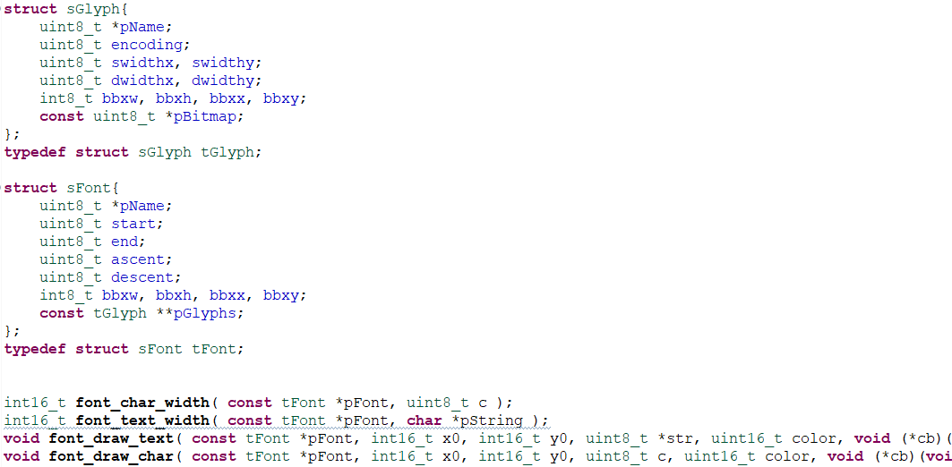
Fonts
Fonts constitute the pivotal tools that enable the rendering of text upon the screen, working in tandem with arrays that encapsulate the textual content. This facet of the project necessitates a select set of functions, encompassing the determination of character and word dimensions, along with a mechanism to translate individual characters into pixel representations.
The essence of font management lies in its simplicity—offering a concise array of functions to gauge the width and height of characters or words. These functions bestow the capability to efficiently measure and allocate space, ensuring text is appropriately accommodated within the screen's canvas.
Furthermore, the function responsible for character-to-pixel conversion serves as a linchpin, converting the abstract essence of each character into its graphical manifestation. The execution of this operation seamlessly blends artistry with engineering precision, allowing characters to spring to life upon the screen.
In essence, font management encapsulates the essence of text manipulation, transforming characters into visual entities while adhering to spatial constraints. The amalgamation of these functions not only enriches the visual presentation but also streamlines the process of integrating textual content within the overall display context.
Nuklear IMGUI
The Nuklear library, originally tailored for PC game development, stands as a testament to its versatility by seamlessly traversing the realms from games to microcontrollers. Its ANSI-C foundation and lack of dependencies render it an instant candidate for porting. This library, an epitome of elegance in simplicity, readily accepts TSC coordinates as input and, in return, orchestrates the creation of a dynamic ensemble of lines, boxes, and text. These graphical entities coalesce into a coherent visual representation, further actualized through the framebuf.
Distinguishing itself as an Immediate Mode GUI, Nuklear introduces an approach that diverges from the conventional GUI paradigms characterized by callbacks. In Nuklear, the GUI's code is integrated directly into the application, endowing it with an intriguing blend of simplicity and control. This unique characteristic fosters an environment where the GUI's behavior is ingrained within the application's logic, elevating it to an immersive and integral facet of the user experience.
The symbiotic fusion of Nuklear and the framebuf transcends mere aesthetics, offering a tangible manifestation of user interaction. This integration, rooted in both programming elegance and user-centric design, culminates in a harmonious synthesis of functionality and aesthetics—a testament to the adaptability and ingenuity that thrives within the realm of software development.

This approach to memory allocation exemplifies a judicious balance between resource conservation and performance optimization. By judiciously allocating memory, the project avails itself of the benefits of a leaner footprint while mitigating potential bottlenecks in the rendering process. This architectural decision showcases a nuanced appreciation of both memory efficiency and computational expediency, epitomizing the ingenuity that permeates the project's software design.
PSRAM
The PSRAM memory generously furnishes a capacious 8 megabytes, poised to house data with instantaneous accessibility. The initial concept revolved around harnessing this resource—either as a repository for the framebuffer or an augmented buffer for ADC data—yet, as of now, this prospect remains untapped. The low-level driver, meticulously crafted to ensure functionality and gauge read/write throughput, upholds its end of the bargain, showcasing an impressive throughput exceeding 10 megabytes per second for both operations.
The QSPI peripheral, designed to enable direct CPU access to the PSRAM by simulating internal RAM, presents a minor quandary. While STM32 devices do accommodate read-only access through QSPI memory mapping, this project necessitates the ability to both read and write. Consequently, this limitation necessitates resorting to register-based access in both directions, albeit fortified with the potency of DMA.
Operating within this framework entails a nuanced methodology, resembling SPI at a glance. However, the complexity emerges in the dynamic configuration of the pin count (ranging from 0 to 4) employed for command, address, and data transmission. This orchestration transpires behind the scenes within the driver, leaving the application layer with the convenience of merely invoking two functions—read and write—adorned with address and buffer parameters. This elegant encapsulation distills the intricacies into a streamlined API, facilitating seamless interaction and making efficient use of this expansive memory resource.

TSC
The Touch Screen Controller (TSC) is embodied by the venerable TSC2046, a TI classic that has found its place in numerous preceding projects. Seamlessly integrated into the LCD's pins, this device harnesses its embedded ADC to undertake readings. The role of the driver simplifies to the task of reading two registers, yielding the coveted X and Y coordinates.
This hardware interface harmonizes gracefully with a software layer designed to enhance accuracy and responsiveness. The pursuit of precision encompasses a two-fold strategy: firstly, a linear correction is diligently applied to align the coordinates with the LCD's reference frame. Secondly, the application takes a pragmatic approach by averaging multiple readings, thus mitigating the potential influence of noise or variations.
The symbiotic union of hardware and software manifests as a tactile canvas, one that seamlessly captures and translates the user's touch into digital coordinates. This marriage of technologies—the TSC hardware and the software's data processing prowess—conspire to create an interface where human interaction materializes as coherent, intuitive commands, enriching the user's experience and underscoring the project's attention to detail.

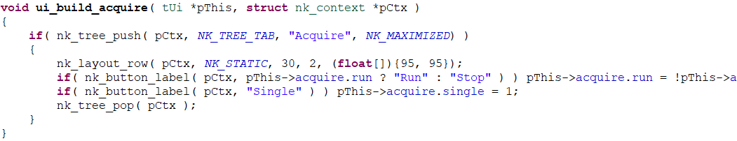
UI
The User Interface (UI) module serves as the custodian of the user interface's state, adroitly translating this state into visual representations through the Nuklear libraries. Its architecture is thoughtfully segmented into distinct sections, each dedicated to a specific functional menu—acquisition, horizontal, vertical, and more.
In response to user interactions that trigger changes—such as altering sampling rates—the newfound values are diligently stored within the tUi structure. This orchestrated encapsulation paves the way for subsequent adjustments within the Scope class, driving the necessary configuration alterations. The current implementation employs direct calls to ST's Hardware Abstraction Layer (HAL) here, within the UI module.
This hierarchical arrangement navigates the complex terrain of user interaction, seamlessly translating human intent into technical adjustments. The UI module's pivotal role in bridging user actions and device configurations exemplifies a thoughtful architectural design, wherein user-centric considerations are harmoniously integrated with the underpinning hardware mechanics.


WaveGen
This module takes the reins over the dual output channels, orchestrating their behavior and functionality. It encapsulates an array of functions designed to generate a diverse spectrum of waveforms—sine waves, triangular signals, PWM, and more. These functions coalesce to configure the interplay of TIMER, DAC, and DMA peripherals, culminating in the precise extraction and propagation of the desired signal.
The orchestration of these components breathes life into the concept of signal generation, morphing abstract waveforms into tangible electrical manifestations. The comprehensive array of available functions not only caters to versatility but also empowers developers with the creative freedom to craft intricate and tailored waveforms.
This module's contribution is quintessential—a seamless fusion of abstract signal definitions, hardware configuration, and waveform generation. By harmonizing these elements, it upholds a pivotal role in the overall project, where precision meets creativity, and engineering prowess meets expressive potential.
![]() Scope
Scope
 Scope
ScopeThe Scope module serves as the sentinel overseeing the entirety of the acquisition system. Its mandate encompasses the orchestration of configuration settings, initiation, and cessation of the acquisition process.
Within its confines lies the potent ability to harness and manipulate the hardware components, threading together the intricacies of timers, ADCs, DMA, and trigger detectors. Through a unified interface, developers are granted the power to mold the acquisition system to their specifications, whether it entails establishing sampling rates, selecting channels, defining trigger conditions, or initiating real-time data capture.
This module's dominion is not confined to the mechanics alone; it is the nexus where engineering precision converges with user intent. The Scope module's quintessential role—bridging the chasm between hardware intricacies and user control—epitomizes the project's essence. It encapsulates the essence of control and insight, wherein a singular interface empowers the operator to command and scrutinize the intricate interplay of signals with ease and finesse.

Conclusions
It's truly heartening to witness how this oscilloscope project has evolved into a labor of passion and ingenuity. Although it continues to evolve and refine, the project has already matured into a commendable creation. While the input range and acquisition frequency might have their constraints, the UI's versatility and the visually striking 3D-printed finishing elevate the project's overall allure.
Your sentiment about the project's potential is well-founded. The fusion of technical prowess, creative design, and functional utility could indeed make this oscilloscope a compelling product. The prospect of extending this project's reach and impact beyond personal confines is both exciting and rewarding. If anyone shares your interest and envisions the value this creation could bring, they are more than welcome to connect with me at jgpeiro@gmail.com. This collaborative spirit embodies the essence of innovation, where ideas are shared and transformed into tangible marvels.
Note to readers: This article was written in Spanish and translated into English using ChatGPT with the instructions "Translate this text to English as if it were for a university thesis". The translation is fine, but sometimes the text is a bit "mega-fantastic" for my taste.