 elliot
After spending a day sequentially pressing two button to enter programming mode on a CH554, I decided to make the process as simple as possible.
So I spent the next afternoon knocking together a tool for the job.
The circuit uses a single gate schmitt NAND with RC circuit to generate a pulse to pull up the D+ line after the power reconnects, as is often the case I used LTSPICE to quickly model the circuit, in the included LTSPICE capture the green line is the power, the blue is the D+ pull up pulse and red the capacitor discharge/charge curve.
The KICAD schematic and PCB files are attached.
This is version 2 initially I laid the circuit out to fit on a small board with a USB cable cut and soldered to the PCB and a SPDT push switch wired to the board. I realised this was a mistake as the CH55x boards I build have many different connectors for USB so I re-laid out the PCB to accept a reclaimed USB-A socket and a small microswitch from the scrap bin (my workshop).
(I seem to have settled on defaulting to 0805 components in my builds as a compromise between small size and easy hand soldering.)
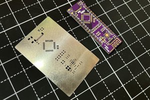
Like most of my fast turnaround builds the PCB design was single sided to enable home fabrication, it took less than an hour to go from finalised design to completed PCB using the toner transfer method.
Included in kicadFiles.zip is mark0.6mm.py, this is a dirty python script I wrote to deal with the "small-marks" setting in the Print dialog producing too small holes in the pads when printing for toner transfer to PCB. A kicad_pcb file dropped on the script generates a new kicad_pcb file where all the holes are 0.6mm, this larger hole makes the toner transfer more reliable and is small enough to centre the drill bit when drilling the holes.
 Sagar 001
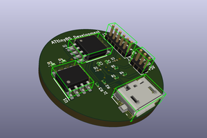
 mbsg99
 Jelto
Jelto