Close
0%
0%

ZX81 logic in six SPLD chips, by Andy Rea

ZX81 logic in SPLDs that are more commonly available than the Ian Bradbury design

Similar projects worth following
Uses two 20V8 and four 16V8 chips (both readily and cheaply available), and a '374 latch.

VSHF.PLD and ZXDECOD.PLD are 20v8.
ZXFERD.PLD, ZXLNC2.PLD, ZXNMI207.PLD and ZXSTATE.PLD are 16v8.

Circuit diagram lost at the moment, but could be largely recreated if you are very familiar with the ZX81 circuit.

I was looking at the Ian Bradbury design and wondering how to port it to more commonplace chips.

Searching the net, I found the remarkable Andy Rea had already implemented the ZX81 logic this way, in 2011.

Much of the information is scattered about the web, and his own pages at http://homepage.ntlworld.com/deborah.clayton1/ULA/ula.html have gone 404.

So I've assembled a collection on hackaday.io for convenience.

I've cached the zipped files from here: 

https://www.sinclairzxworld.com/viewtopic.php?f=6&t=445 (attachment ula2.zip)

No circuit diagram yet but you could probably start from my guess at Ian Bradbury's circuit  and gradually rework it.

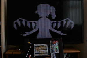
Andy Rea pointed me at Wilf Ritger's articles about ZX81 video text and high-res graphics.
I need to wrap a towel soaked in icy water round my head when I plough through that. :-)

ZX81_logic_in_SPLD_chip_diagrams.txt

Chip pinouts. Needed for recreating the circuit diagram.

plain - 4.90 kB - 10/07/2023 at 13:41

Download

ula2.zip

Logic source code (in CUPL) and JEDEC files etc. You'll need a programmer that can handle 16V8 and 20V8 devices.

Zip Archive - 56.43 kB - 10/04/2023 at 15:50

Download

  • Logic analysis

    Keith10/15/2023 at 01:46 0 comments

    2023-10-14

    After a lot of reading and feeling like D.P. Gumby saying "My brain hurts!", I've now got a better grasp of what is going on.

    I started from Andy's ZX81 logic in TTL. You might think "surely that is just a ZX80" but it is isn't. The ZX81 had to pull many tricks to fit the logic in a 40-pin ULA. Extensive "resistorplexing" of course, but it also had to make do with a limited number of Z80 signals. The ULA had to find different ways to know where it was in the video display cycle.

    Andy's TTL replacement for the ULA used a state machine based on a 3-bit counter, reset at the start of /M1 and clocked twice the CPU clock rate. The logic can then know where it is in eight phases  of T-states 1 to 4.

    In the ZX80, the video character latch is loaded at the end of /MREQ when not refreshing, and read when /RFSH and /MREQ are low.

    In Andy's TTL ZX81 logic, the video character latch is loaded at the end of T2, and read during T4.

    For character text display, the video character latch drives address lines of the font ROM.

    For G007 graphics display, the process is very similar but the latched video data is read straight to the data bus without having to go through the font ROM. I think the load and read signals could share the same timing, but with the font ROM disabled during G007 graphics and vice versa. This bodes well for integrating G007 graphics into Andy's logic.

    2023-10-15

    Andy's state machine seems to begin by clocking in /M1, which falls slightly after the start of T1. 

    I am not sure about the start and end conditions, but the display process is the above repeated 32 times. So the end of one becomes the start of the next.

    Andy's logic seems the best for TTL implementation.

    I wondered if the state machine in GAL chips could be optimised like so:

    Here the state machine includes the latch's clk and oe signals, which saves needing separate pins.

    The machine stays in state 5 (idle) unless /M1 is low, in which case it cycles through states 4,6,3 and 5.

    The latch output may only go low for video cycles, so the simplest fix may be to clock /M1 in during video display (A15 and A14 are high).

    2023-10-19

    After correspondence with Andy, I see I have made two errors

    • Andy's state machine enters state 0 asynchronously as soon as /M1 falls.
      So the timing begins half a clock earlier.
    • ZX81 ULA replacements have to load the character latch BEFORE forcing NOP on the data bus, 
      unlike the ZX80 which does both at the same time.

    Thus the timing looks more like this:

    The forced NOP has to straddle the end of T2. It needs some delay to allow the data hold time of the data latch, and some delay between releasing NOP and the data latch output enabled.

    One can do this with gate delays, or double the clock resolution and have the forced NOP just a quarter of a CPU clock cycle either side of the end of T2. Andy says his Xilinx version of the ULA does the latter.

View project log

Enjoy this project?

Share

Discussions

Similar Projects

Does this project spark your interest?

Become a member to follow this project and never miss any updates