 Viktor Nikolov
Motivation: Why MicroZed?
I'm an electronics enthusiast who got fascinated by FPGA and AMD Xilinx Zynq-7000 System-on-Chip. I found that great development boards exist for Xilinx Zynq-7000, allowing you to explore and play with the platform (for example Zybo Z7). But how do you use Zynq-7000 "in the field" on the final HW device you built? A development board like Zybo Z7 (12 cm x 9 cm) is not very practical for such purposes and is not meant to be used like that.
For Arduinos, ESP and other micro-controllers, you can choose from an extensive offering of small-factor breakout boards, which you insert or solder into your own HW. Unfortunately, I discovered that in the world of Xilinx Zynq-7000, the offering of non-development boards is limited.
After doing some research, I decided to use Avnet MicroZed in a hobby project of mine. This System-on-Module was introduced into the market back in 2013. Avnet did the last revision at the end of 2020, so I hope MicroZed will still be available for some time. It's a relatively compact board (10 cm x 6 cm), comes with very detailed documentation, and one of its perks is the Ethernet interface (important for my project). There are two versions of the MicroZed. One is using Xilinx Zynq-7010 SoC, and the other uses Zynq-7020 SoC.
Please note that to program the MicroZed board, you will need a JTAG programming cable (I recommend Digilent JTAG-HS3 Programming Cable).
Banks, voltages and power-up sequence
Another difference from the microcontroller breakout boards is that you can't just plug the MicroZed into your PCB and start using its I/O pins. The concept of MicroZed SoM is that you plug it into a "carrier card" which provides: 1) circuitry necessary for the MicroZed I/O pins to function as expected; 2) peripherals to be connected to the MicroZed (i.e., the circuitry because of which you created the project in the first place)
Your carrier card has to provide power to the MicroZed I/O pins. This is to give you the flexibility to choose a voltage level for I/O pins to operate on. I/O pins of Xilinx Zynq-7000 are organized into "banks". Banks are identified by numbers. MicroZed provides 53 pins from the Bank 34 and 53 pins from the Bank 35. The more expensive version using the Zynq-7020 chip provides an additional 16 pins from the Bank 13.
Each pin bank has its own power rail (designated as VCCIO). VCCIO can provide 1.8 V, 2.5 V or 3.3 V. Selecting VCCIO voltage is a crucial design choice. For basic low-speed I/O, 3.3 V is OK (e.g., connecting components to the Zynq by SPI). But if you need more advanced stuff (e.g., using fast differential signals), you must select 1.8 V or 2.5 V because Zynq-7000 can't do differential signals on 3.3 V (you can check this Xilinx support article for details).
In addition, you have to ensure proper power-up sequence. First, the power rails on the MicroZed start. When done, the signal VCCIO_EN provided from the MicroZed to the carrier card goes high. Only then can the VCCIO rails for the Banks 53/54/13 start. When the VCCIO voltage stabilizes, the carrier card sets the "power good on carrier" signal (PG_CARRIER) high, which goes back to the MicroZed.
Basic design decisions
So, I knew I wanted to use the MicroZed in a project, and thanks to its detailed documentation, I became aware of the complexities explained in the previous chapter. Therefore, I decided to build a development carrier card as a "teaching case" and use the gained experience later when designing a future project's PCB, which will "carry" the MicroZed.
I chose to design the board from the beginning with the intention of having it professionally assembled at a factory. My soldering skills do have limits, and I knew there would be tiny components difficult to solder manually (I don't have a reflow oven nor experience using a hot plate). For example, the two 100-pin BergStak connectors between the MicroZed and the carrier card have soldering...
Read more »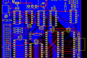
 Keith
Keith
 Nick Sayer
 Ken Yap