deʃhipu
-
Learn Inkscape
09/13/2017 at 12:21 • 2 commentsIf you want to do anything more advanced with Fritzing — design your own footprints, use custom-shaped PCBs, panelize your designs, etc. — you are going to need to edit SVG files. Fritzing itself doesn't let you do that — the authors figured out that any crippled editor they can make will be infinitely inferior to the general-purpose graphics editors made by dedicated teams. So they rely on you using an external editors. Inkscape is one particularly nice graphics editor that edits SVG files natively and lets you do a lot in a very convenient way. It has grids, rules, automatic arrangement of objects, measuring and even lets you edit the XML attributes of elements directly. So the very first tip I have for getting the most out of Fritzing is installing and learning to use Inkscape.
-
Vero and Proto Boards
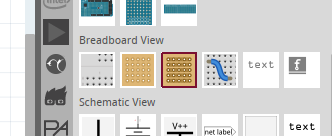
09/13/2017 at 12:28 • 0 commentsOne unique use case for Fritzing that is not well supported by other CAD software is designing your prototypes. You are probably familiar with the breadboard view that Fritzing presents to you by default. But did you know that you can delete the breadboard from it, and instead drag a perfboard (protoboard) or a stripboard (veroboard) from the palette, and use that?
![]()
The stripboard object also lets you make connections and gaps between the individual holes by clicking on the space between them. That's perfect for planning where to cut the copper strip. You can also re-create any custom layout of a prototype board that you happen to have — there is even a Radio Shack 276-150 layout available in the drop-down menu.
You don't like to use the prototyping boards, and instead prefer to do stuff dead-bug style? No problem, you can do that too! Well, maybe not in 3D, but at least you can plan your work a little. The fact that Fritzing has graphics for how the parts actually look like helps with that greatly.
You can even have several breadboards, perfboards and stripboards in your project at the same time!
-
Hole Sizes
09/14/2017 at 14:43 • 0 commentsWhen Fritzing was created, we didn't have anything like OSHPark, and most hobbyist were making their PCBs manually at home. That included drilling. That's probably why the Fritzing defaults to 1mm hole sizes with a preety wide copper circle around them — it's simply much easier to do by hand.
But today, when we send our PCBs to fabricators who use automated processes for everything, it doesn't make much sense, and the huge holes and pads mean it's impossible to route a track between them.
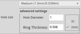
Fortunately, you can change the sizes of holes for your headers, using the "hole size" settings:
![]()
You have three pre-sets, but you can also enter your own numbers, and they will be remembered as one more preset. Personally I like using 0.9mm for the hole diameter and 0.4mm for the ring thickness — this gives pretty good fit for the male headers, with enough copper to solder them to, and enough room between the pins to fit a trace comfortably.
-
Mystery Part
09/14/2017 at 14:49 • 0 commentsSometimes you have some module or part that you want to use in your project, but since it's just a one-off, you don't feel like making a special footprint for it. You could just use pin headers for it, and that's what I usually did, but there is a better way: a mystery part.
![]()
It looks like a black box with a question mark on it, and it's basically a pin header with some extra options. What are the extras? Well, first of all, it has the first pin marked with a square — so that you know how to rotate your part. But more importantly, it has that "edit pin labels" button, which lets you assign names to all of the pins, so that when you hover over them with mouse, you can see what they are. This makes it much harder to make a mistake when connecting everything.
It also looks like a plain box in the schematic view, better than the anonymous headers. Of course you should give it a label describing what it actually is.
-
Ratsnest Lines
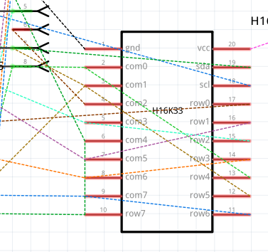
09/15/2017 at 07:47 • 0 commentsOne of the nicest features of Fritzing is that it lets you easily switch between the schematic and PCB views, and the updates you make in one will show in the other in the form of so called "ratsnest" lines — color dashed lines.
![]()
However, while generally useful, they can become very problematic when too dense, because of one peculiarity of Fritzing — the ratsnest lines have clicking priority over everything else, so it may be very difficult to click on anything covered by them. A quick workaround is to double-click on the offending lines to turn them into traces, which obey normal clicking priority rules and are not as problematic, but then it's hard to keep track of what you have already connected in your design.
A better way is to simply disable the display of the ratsnest layer. You can do that in the menu, by clicking on the checkbox next to View→Ratsnest Layer. But then how are you going to know what to connect to what? Don't worry, if you click on any pin, Fritzing will highlight all the other pins it should be connected to — this way you can make all your connections while avoiding visual clutter.
Though I still wish there was an option of making the ratsnest lines unclickable...
-
The Grid
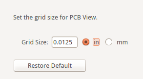
09/15/2017 at 08:04 • 0 commentsThe grid is a very useful tool. It lets you align all your parts properly, and make sure the traces between them are straight. However, the default grid in Fritzing is set to a huge 0.1" — which is probably fine for large through-hole parts, but completely inadequate for the smaller SMD components. Fortunately you can change the grid size using the View → Set Grid Size... menu option:
![]()
I usually start with a pretty large grid, such as 0.05", and then halve it whenever I need more detail or denser traces. This lets me make sure that all the large parts are properly aligned to the bigger grid, but the traces can still go around them.
You can also temporarily disable snapping to the grid with the menu option View → Align to Grid, or by holding down the Ctrl key while moving a trace. This can be useful for those few traces that don't want to align no matter what you do, because the footprint you are using is not compatible with the grid you have set.
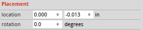
Another trick is to hold down both Ctrl and Shift keys while moving a trace — then it will automatically snap to horizontal, vertical or diagonal positions. I use that to connect traces to the pins of small integrated circuits, which somehow never align with my grid. So I make the first segment of the track horizontal, until it crosses the grid, and from there it all aligns properly again.
Some objects, like the PCB itself or images, will never snap to the grid for some reason. To align them perfectly, you can use the "location" and "rotation" properties. This is also the way to get a rotation that is not a multiple of 45°.
![]()
-
Rotating Everything
09/17/2017 at 16:59 • 0 commentsRotating elements is easy. You just use the "rotate" button in the bottom left corner of the screen, right?
![]()
Well, yes, you can do that and that works fine most of the time. But there are limitations. By default, that button rotates things by 90°. Some objects can be rotated by 45° by clicking on the small arrow on that button, and selecting the appropriate option for the pop-up menu. But some things, such as vias and holes, can't be rotated at all. Initially that makes sense. After all, why would you want to rotate a round hole or via — they look the same no matter how they are rotated! However, you might still need to rotate a set of holes or vias, or a mix of parts (like your whole design, for example) that includes holes and vias in it. And Fritzing won't let you do that.
I had this problem with an Adafruit Feather shield that I was designing — it's slightly longer than 5cm, but my board house would only make 5×5cm boards cheaply, anything larger costs extra. But I figured out that I can fit this shield into the 5×5cm outline if only I rotate it by 45°. But how can I do that when it contains vias and holes?
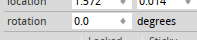
Looking for a way to do this, I found this "rotation" property in the side pane:
![]()
This lets you rotate a single object by pretty much any angle, not just multiplies of 45° or 90°. In particular, you can rotate your PCB by any amount, even though that red button only lets you do 90° for the PCBs. Neat! But I can't use that when I have multiple objects selected, so it doesn't solve the problem.
I wish I could also figure out the next piece of the puzzle myself, but I actually found it on the Fritzing's user forum. You see, the PCB has one property that other objects don't have — the "sticky" checkbox, right under that rotation property:
![]()
When an object is sticky, whenever you move it, it will also take with it all other objects that touch it. And rotation counts as movement here. So all I had to do is make my PCB sticky and set its rotation, and everything on it rotated together with it. Presto!
Of course, sometimes you want to just rotate a few selected parts. Then you can drag a second PCB onto your design, make it sticky, put all the parts you need rotated on it, rotate it, and then delete the PCB and move the parts back where you need them. A bit hacky, but workable.
-
Part Libraries
09/17/2017 at 17:52 • 0 commentsFritzing comes by default with a pretty large library of parts that you can use in your designs, and new parts are being added to that library all the time by various contributors. However, there are also a few large part libraries outside of that, that you might want to add to your installation. The biggest ones are probably the libraries of parts made by the companies that sell those parts:
See the README in the Adafruit's library for detailed instructions on adding those to your Fritzing.
-
Trace Aesthetics
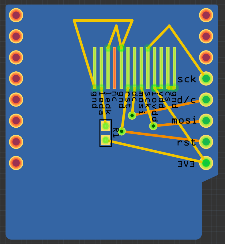
09/18/2017 at 10:37 • 0 commentsI've been putting this post off for some time now, but we need to talk about this sooner or later. Fritzing became infamous in the electronics community for the characteristic ugly traces that are often done with it. People new to the whole thing just connect the holes and pads in straight lines, adding a bend sometimes when necessary, and call it a day. It looks something like this:
![]()
What's wrong with this, you ask? All the connections are there, so it will work fine, after all, no?
Well, there is a number of things wrong. First of all, you are just being lazy, and that's a sure warning sign that most likely there will be other problems with this design. Second, this is not pleasant to look at, and more importantly, to work with. It's not easy to see what is connected where and to modify this design. It's also easy to miss shorts between the traces. Finally, there are actual technical reasons why this design is sub-optimal.
You probably have heard about radio-frequency emissions from traces. Turns out that every trace is basically a small antenna, and it will waste energy by emitting radio waves. Most traces are not particularly good antennas, but the ones that have a lot of sharp angles and are not surrounded by copper fill are better at emitting noise. Unless you are working with gigahertz signal, this is not the technical reason for worrying about sharp angles, though.
If you are etching your own boards, you have to be very careful about all the nooks and crannies in your design. The etchant will tend to pool int them, and eat out much more copper in those places, leading to possible faulty boards. This is not the technical reason for worrying about sharp angles if you send your design to a professional board house for fabrication, though. Neither is the fact that because of the lack of a copper fill, a lot of copper has to be etched away and a lot of the etchant wasted on that, and the etching process will take a lot of time.
Finally, the sharp corners are more likely to peel off the board, especially if it's subject to any mechanical stresses or bad storage. Again, not much of an issue with professionally made boards.
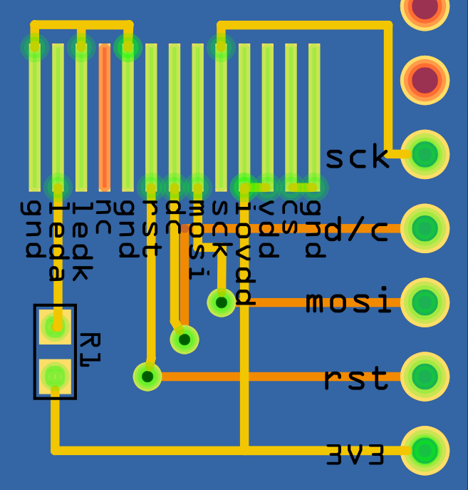
But it still looks very bad, and all the people who ate their teeth on the above-mentioned limitations will shudder at the sight of it. So please, be a nice person and spend the minimal extra effort to actually make it look good. Start by aligning all the traces so that you only have horizontal, vertical and diagonal lines (you can hold ctrl+shift while moving the trace for Fritzing to help you with it):
![]()
Much better already, don't you think? Now let's get rid of those sharp angles:![]()
It's starting to look right, doesn't it? Note that I actually left a couple of right angles in there — in the T-junctions, and also for the traces that are too close together to actually do a nice gradual turn. Personally I think this is fine, but for the reasons I listed above, opinions vary. Finally, let's add a copper fill:
![]()
Et voila! A decent looking PCB design. It wasn't so difficult after all, was it?
Of course there is much more to it than just the horizontal and vertical lines and sharp angles. But this is already a start. If you keep practicing, looking at other people's designs, etc. you will come up with your own set of good habits that make the designs nicer, easier to read, less likely to contain mistakes, and more pleasant to work with.
-
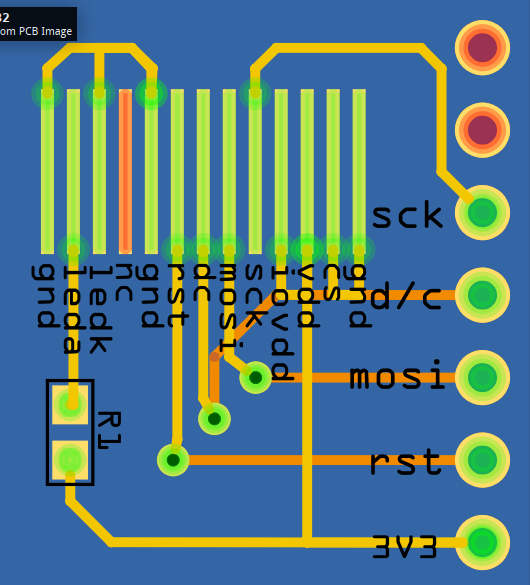
Net Labels
09/24/2017 at 19:19 • 0 commentsLet's talk a little bit about schematics. I know that you rarely visit that tab, but if you want other people to actually make sense of your project, you have to document it. Like I did with my #D1 Mini Matrix Shield:
![]()
I really tried to make it readable. However, the LED matrix has such ridiculously random pinout, and there are so many connections, that it's really difficult to make sense of it.
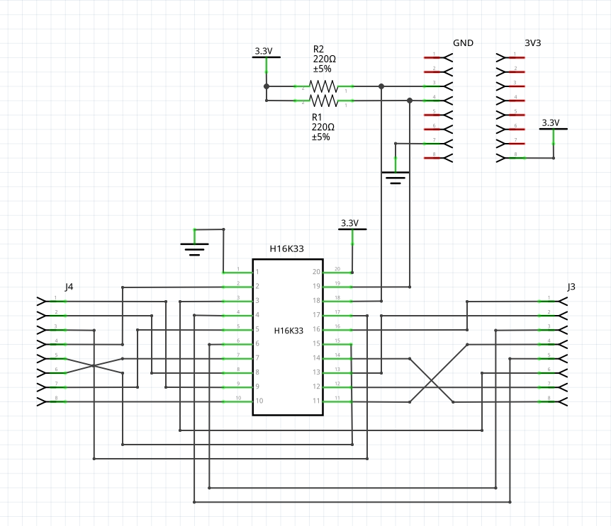
Today I'm a little bit wiser and I use the net labels, which you can find in your parts pane under schematic view:
![]()
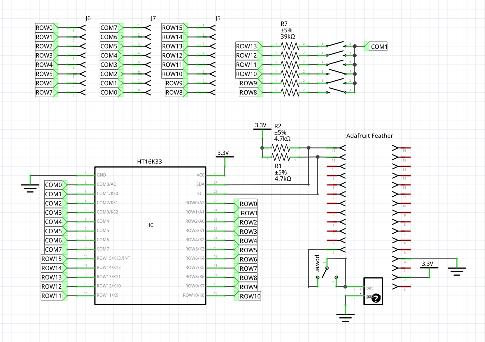
The way you use it, you connect it in place of a wire, and at the other end you make another one, with the same name. Fritzing considers all the labels with the same network name on them connected. The resulting schematic is much easier to read, like the way I made for #PewPew FeatherWing:
![]()
Of course, this is not a silver bullet. If you overdo it, and all your connections are just some random labels, your schematic will be even harder to read. But if you can think of a name for a given connection, it's probably a good idea to use a label for it.