Close
0%
0%

The Hobbyists Guide to FPGAs

Follow this project to learn how to use FPGAs and incorporate them into your projects.

Similar projects worth following
The Hobbyists Guide to FPGAs is project created to host practical tutorials, theory of design articles, and hands-on labs all in the name of guiding hobbyists through the wonderful world of FPGAs.

If you are curious about FPGAs and want to know more, or if you have your own FPGA boards already, then come along for the ride and follow this project. New material will be posted using the project log mechanism and will appear on your feed. Though most concepts apply to all FPGAs and digital design in general, they will be focused on the TinyFPGA line of FPGA boards.

Introduction

The Hobbyists Guide to FPGAs is a regular blog that will constitute a book by the time it has run its course.  As more log entries are added they will be added to the table of contents below.  Possible future topics will be added to the table of contents without a link.  New log entries will generally follow these future topics, but there are reasons why it may not always be so.

The best way to read the most up to date logs and implement the latest labs is to follow this project on hackaday.io.  As each new article, tutorial, and lab is added you will receive a notification in your feed.

Table of Contents

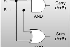
  • Introduction to Verilog and Combinatorial Logic

    Luke Valenty10/05/2017 at 05:00 11 comments

    Introduction

    There are three primary methods for developing FPGA designs:

    1. Verilog
    2. VHDL
    3. Schematic Capture

    The Hobbyist's Guide to FPGAs will focus on using Verilog to program FPGAs. Verilog and VHDL are both hardware description languages.  They allow you to design digital logic circuits by describing them in their language. Verilog was chosen for this guide because it has an easier learning curve and is not quite as picky as VHDL is.  There are some that would argue for using VHDL, and for good reason.  VHDL has some powerful constructs that Verilog does not.  For the average hobbyist, however, Verilog is the right choice and will provide a more pleasant entrance into the world of FPGAs.

    Verilog

    When designing any system, it is useful to be able to decompose the problem into smaller parts.  Digital design is no different.  In Verilog we have the concept of modules.  A module is a self-contained design that communicates externally through ports.  The ports on a module are input and output wires.  You could think of a module as it's own standalone logic chip.  When we are developing a new design, we start with a module.

    /*
     * Implements a simple 1-bit half-adder.
     */
    module half_adder (
        input a,
        input b,
        output sum,
        output carry
    );
        // sum is the xor of the two inputs
        assign sum = a ^ b;
        
        // carry is true only if both inputs are true
        assign carry = a & b;
    endmodule
    

    The above example is a reusable module that implements a half-adder.  It's a nice and simple example that illustrates a few fundamental attributes of Verilog:

    1. All functionality is implemented within modules.
    2. Module ports have an associated direction.
    3. We can directly assign expressions to ports and wires.
    4. Expressions and comments in Verilog are very similar to expressions and comments in C, C++, and Java.

    The assign statement performs a continuous assignment.  It's not assigning a singular value to the left-hand side.  Instead, it is assigning an expression to the left-hand side.  If the value of any components of the expression changes, then the value of the left-hand side wire will change as well.  The text of the Verilog translates directly into digital logic elements.  If we designed the module as a schematic it might like similar to the one below:

    This is an accurate schematic of what the half adder module might look like if it were assembled with logic gates.  FPGAs, despite their name, don't actually use logic gates.  Instead they use much more powerful LUTs, or Look-Up Tables.  In the actual FPGA implementation, the module would look more like the following diagram:


    Instead of specific logic gates, the outputs of sum and carry are generated by the LUTs present in the FPGA fabric.  The LUTs are programmed to behave like an XOR gate and an AND gate.

    Modules can be reused in other modules.  We can take our half adder and use it to create a full adder.

    /*
     * Implements a 1-bit full-adder.
     */
    module full_adder (
        input a,
        input b,
        input carry_in,
        output sum,
        output carry_out
    );
        // carry outputs from half adders
        wire carry_1;
        wire carry_2;
        
        // intermediate sum from first half adder
        wire sum_1;
        
        // instantiate the first half adder
        half_adder ha_1 (
            .a(a),
            .b(b),
            .carry(carry_1),
            .sum(sum_1)
        );
        
        // instantiate the second half adder
        half_adder ha_2 (
            .a(sum_1),
            .b(carry_in),
    ...
    Read more »

  • What are FPGAs?

    Luke Valenty10/02/2017 at 07:10 1 comment

    FPGAs and Microcontrollers

    FPGA is an initialism for Field Programmable Gate Array.  They are digital logic chips that can be programmed with new logic designs in the same way that microcontrollers can be programmed with new firmware.  On a microcontroller, a program is a series of instructions the CPU executes one at a time.  Each instruction takes time to execute, program memory to store, and may access locations in RAM.  

    Designs for FPGAs are different from programs in microcontrollers.  The design defines a series of digital logic circuits, the connections, RAM and ROMs they may use, multipliers, etc.  Each element of the design consumes a physical location of the FPGA.  In a microcontroller instructions are executed one at a time.  In an FPGA all elements of the design can be active at once.  This makes FPGAs very powerful.  In fact, an FPGA can implement a microcontroller in addition to custom logic.

    Architecture

    Inside many modern FPGAs there is an array of 4-input logic function generators, single bit storage elements, and other small bits of general purpose logic connected by a routing matrix.  The image below is what a logic slice from the MachXO2 FPGA in the #TinyFPGA A-Series boards looks like.

    MachXO2 FPGA Logic SliceMachXO2 FPGA Logic Slice. From the MachXO2 User Guide - http://www.latticesemi.com/view_document?document_id=38834

    Rather than using individual 2-input logic gates, the LUT4 logic function generators or Look-Up Tables can generate any 4-bit logic function.  The output of the logic generator can either be routed to another LUT4 elsewhere, or can be stored in the D Flip-Flop immediately connected to the output of the LUT4.  

    Many FPGA architectures group slices into larger elements.  In the MachXO2 series from Lattice they are called PFUs, or Programmable Function Units.  Since addition, subtraction, and comparison operators are so common, there is an optimized carry-chain between neighboring slices that allows for faster execution of such operations.  

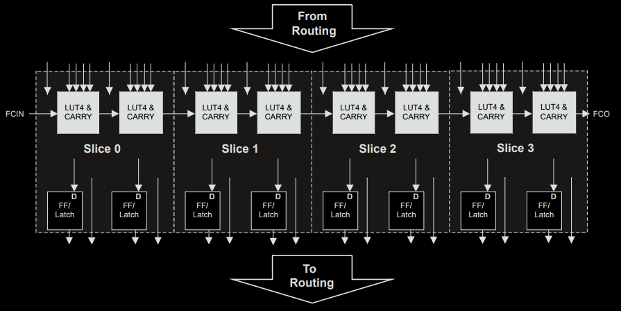
    MachXO2 FPGA Programmable Function Unit. From the MachXO2 User Guide - http://www.latticesemi.com/view_document?document_id=38834

    Between the PFUs is a routing matrix with many wires and switching matrices that allow for connections between PFUs and other components in the FPGA.  In addition to the PFUs, FPGAs may contain other modules like RAMs, clocks, PLLs, non-volatile memory, and even hard-coded peripherals like SPI and i2c masters and slaves.  The picture below is the basic layout of the MachXO2-1200 FPGA in the TinyFPGA A2 board.

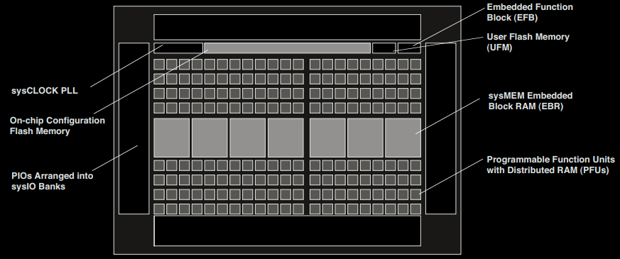
    MachXO2-1200 FPGA Top View. From the MachXO2 User Guide -http://www.latticesemi.com/view_document?document_id=38834

    Programming

    Every programmable element within an FPGA stores is programming locally.  The LUT4 function generators for example contain 16-bits of information.  The 4 bits of input can be interpreted as a numerical index into that information and the output is the value at that location.  All of the routing programming contains storage bits that define how the design connects the various components.  This configuration is stored in volatile storage elements.  When the power goes off, they lose their state.

    This means FPGAs need to be reprogrammed every time they power-on.  Luckily there are automated mechanisms for FPGAs to load their configuration from an external flash memory, or even an internal flash memory on power-on.  

    In the #TinyFPGA A-Series this configuration flash is built into the FPGA itself.  In the #TinyFPGA B-Series boards this configuration flash is on a separate SPI flash chip integrated on the board.  Once a design is synthesized, it can be programmed onto the configuration flash on the board.  

    Developing for FPGAs

    FPGAs come in chip packages that are difficult to integrate into hobbyist projects.  Therefore there are development boards for FPGAs that...

    Read more »

View all 2 project logs

Enjoy this project?

Share

Discussions

Madeline Thom wrote 11/13/2019 at 10:10 point

This is a very cool project, I think many students will like it.

  Are you sure? yes | no

Similar Projects

Does this project spark your interest?

Become a member to follow this project and never miss any updates