Close
0%
0%

FPGA Bootcamp #3

Put your Verilog on real hardware, real cheap

Similar projects worth following
In the first two bootcamps you developed a simple demonstration app and simulated it. Now it is time to put it on a real piece of hardware. The Lattice IceStick which is very inexpensive and easy to use will host your demo nicely. Along the way, you'll learn how FPGAs are configured, how to use open source FPGA tools, and how to assign real hardware resources to your designs.

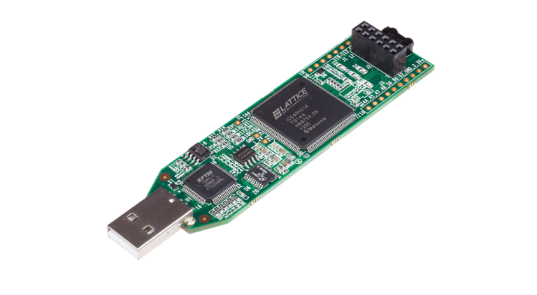
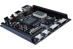
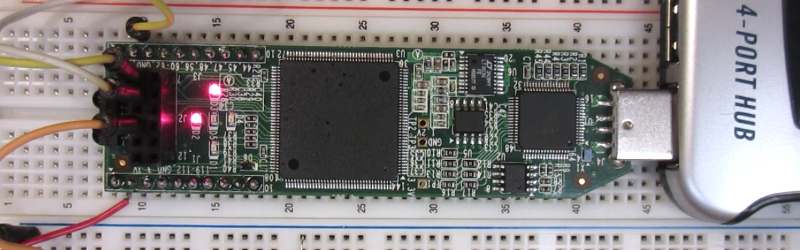
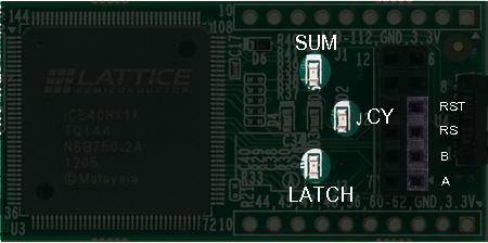
In the last two bootcamps, you developed a simple application and simulated it. That's nice, but you want to see real hardware working. That's what you'll do in this exercise. We'll use a $20-something board called an IceStick which contains a Lattice FPGA. There's three reasons we are going to use that particular board:

  1. Very inexpensive
  2. Easy-to-use since it just plugs into a USB port
  3. Open source tools that work well

The good news is that the basic workflow will be the same no matter what FPGA you want to use. You'll simply use different tools, so the details will be different. We will use a set of open source tools that include Yosys, Arachne-PNR, and IceStorm (which is a suite of tools).  For simulation, we used EDAPlayground or Icarus in the last two bootcamps. The basic workflow will be:

  1. Synthesize Verilog into low-level constructs (Yosys)
  2. Simulate/test/debug system behavior (EDAPlayground or Icarus).
  3. Map low-level constructs to specific device blocks (Yosys)
  4. Place and route blocks -- this means to plan which blocks go where and exactly how to interconnect them (Arachne-PNR)
  5. High-fidelity simulate/test/debug on actual device-specific configuration (Not covered in this bootcamp)
  6. Program configuration to FPGA or configuration device (icepack/iceprog)
  7. In circuit test/debug, if necessary (your brain and test equipment)

This bootcamp is part of a series:

Bootcamp 0Covers basic digital logic concepts with simulations 
Bootcamp 1Introduction to FPGA coding and simulation with combinatorial logic 
Bootcamp 2More FPGA coding and simulation with flip flops (sequential logic)
Bootcamp 3Working with actual FPGA hardware (this bootcamp)

When you are ready, move on to the steps and continue on your FPGA adventure! You'll also find background articles in the project logs. You might want to browse them first and refer back to them as you work through the steps. The logs also have a glossary you can check for any unfamiliar terms.

icestickfull.pcf

Constraint file for newer versions of Arachne which can ignore unused constraints.

x-font-pcf - 2.41 kB - 07/12/2018 at 19:44

Download

build.sh

Bash script for managing workflow.

x-shellscript - 977.00 bytes - 07/12/2018 at 19:44

Download

icestick.pcf

Constraint file for all versions of Arachne with unused entries commented out.

x-font-pcf - 1.84 kB - 07/12/2018 at 19:44

Download

demo.v

Demo Verilog file.

x-verilog - 2.01 kB - 07/12/2018 at 19:44

Download

  • 1 × Lattice IceStick FPGA board You will need this board to follow along in this bootcamp!

  • Understanding Configuration

    Al Williams07/12/2018 at 20:46 0 comments

    If you start with a C program, you use a compiler and a linker to convert that code into an executable format. You might use one toolchain to generate a Linux executable and another for a Windows EXE. Still another might produce a hex file to put in an Atmel processor. Even though each takes different tools, the process is more or less the same and it is an analog for how we configure an FPGA.

    Whatever tools you use, the workflow for any FPGA is basically the same, although details of the specific tools may vary. Sometimes the names vary a bit, too. Although you write code in Verilog, the FPGA has different blocks (not all vendors call them blocks) that have certain functions and methods they can connect. Not all blocks have to be the same either. For example, some FPGAs have blocks that are essentially look up tables. Suppose you have a look up table with one bit of output and 16 rows. That table could generate any combinatorial logic with 4 inputs and one output. Other blocks on the same FPGA might be set up to be used as memory, DSP calculations, or even clock generation.

    Some FPGAs use cells based on multiplexers instead of look up tables, and most combine some combinatorial logic with a configurable flip flop of some kind. The good news is that unless you are trying to squeeze every bit of performance out of an FPGA, you probably don’t care about any of this. You write Verilog and the tools create a bitstream that you download into the FPGA or a configuration device (more on that in a minute).

    The general steps to any FPGA development (assuming you’ve already written the Verilog) are:

    • Synthesize – convert Verilog into a simplified logic circuit
    • Map – Identify parts of the synthesized design and map them to the blocks inside the FPGA
    • Place – Allocate specific blocks inside the FPGA for the design
    • Route – Make the connections between blocks required to form the circuits
    • Configure – Send the bitstream to either the FPGA or a configuration device

    The place and route step is usually done as one step, because it is like autorouting a PC board. The router may have to move things around to get an efficient routing. Advanced FPGA designers may give hints to the different tools, but for most simple projects, the tools do fine. Synthesize and map are often done in one swoop, also.

    One way to think of this is that someone has given you a printed circuit board with a bunch of components holes already drilled out but all the copper is still on it. So you know a resistor is going to go in these holes and an IC in another set of holes. You can't change that. The synthesize and map steps take your design and figure out how to implement it with the components that are there. Like a schematic, though, that doesn't tell you anything about a component's position on the board or any traces. The board might have 10 resistors and you need 3. The schematic doesn't tell you which 3 you are going to use.

    The place and route steps then take that schematic and determine which components you will make use of and how to etch the copper to form the traces between them. To carry the analogy further, the configuration step is the etching and building of the board.

    Of course, there's no copper and etching involved. That's just an analogy. We'll talk about constraints which can tell the place and route steps that you insist on using a certain component for a certain Verilog construct. That's important when you have, say, a particular I/O pin connected to something and you need a signal to drive it, although there are other reasons you might do it, as well.

    Even though we are talking about a very specific board in this bootcamp, you'll find that if you are using Verilog to configure an FPGA the steps will always be pretty close to this. Some tools will have slightly different names or break the tasks up differently, but all of these tasks will still apply.

    Another common way to configure an FPGA is with VHDL which is another description language. The workflow...

    Read more »

  • A Quick FPGA Glossary

    Al Williams07/12/2018 at 19:49 0 comments

    • Adder - See Full Adder and Half Adder.
    • AND Gate - A gate who's output is 1 only when all inputs are 1.
    • Blocking assignment - In Verilog, when an assignment occurs before any subsequent assignments (that is, it does not occur in parallel).
    • Combinatorial Logic - Logic that does not rely on the previous state of the system to set the current output state.
    • Exclusive OR Gate - See XOR Gate.
    • Flip Flop - A circuit element that can take one of two states (1 or 0) and remember it until changed. Somewhat like a one-bit memory device.
    • Full Adder - A circuit for adding two binary numbers and a carry bit (so three bits overall). It will produce a sum and a carry.
    • FPGA - Field Programmable Gate Array.
    • Half Adder - A circuit for adding two binary numbers. It will produce a sum and a carry
    • Inverter - See NOT Gate.
    • IP - Intellectual Property. Typically a third party module that does a particular function that you can integrate into your FPGA designs if you wish.
    • Logic Diagram - See Schematic.
    • Non-blocking Assignment - In Verilog, when an assignment occurs in parallel with other assignments in the same block.
    • NOT Gate - A gate that takes a single input and inverts it. That is, a 1 becomes a 0 and a 0 becomes a 1.
    • OR Gate - A gate who's output is a 1 if any inputs are 1.
    • Schematic - A diagram of a logic circuit  made up, usually, of logic symbols for fundamental gates.
    • Sequential Logic - Logic that typically uses flip flops and the current output state influences future output states.
    • Testbench - Verilog (or similar) code that exists only to send stimulus to a simulated device and record or test the results.
    • Truth Table - A table showing a logic circuit's possible inputs and the outputs that will result.
    • Workflow - The process of taking design inputs and producing a working FPGA configuration.
    • Verilog - A description language used to describe logic you wish to place on an FPGA.
    • VHDL - A description language (not used in this bootcamp) to describe logic you wish to place on an FPGA.
    • XOR Gate - Exclusive OR gate. A two-input gate that sets its output to 1 if either input is a 1, but not when both inputs are a 1.

    Logic Truth Tables for Two-Input Gates

    ABANDORXOR
    00000
    01011
    10011
    11110

View all 2 project logs

  • 1
    ▇▇▇▇ Get Started ▇▇▇▇

    Reader note: If you would like to view this in the center of the screen, click on the View Instructions tab all the way at the bottom.

    In the previous bootcamps, you built a simple Verilog demonstration consisting of an adder and a few flip flop-based circuits. The simulations work, so now it is time to put the design into a real FPGA and see if it works in the real world. The FPGA board we’ll use is the Lattice iCEstick, an inexpensive ($25) board that fits into a USB socket.

    Like most vendors, Lattice lets you download free tools that will work with the iCEstick. However, they are often painful to install and the Lattice FPGA is one of the few that has a complete Open Source toolchain for Verilog so we're going to use that. The tools have instructions for installing under Linux, Windows, and the Mac. I will use Linux, but the process is essentially the same regardless of operating system.

    Here's our general game plan:

    • Install the tools
    • Assemble our Verilog file and a constraint file -- you can download these from the Files section or Github or you can keep using the Verilog file you've used in previous bootcamps
    • Run 3 programs to produce a bitstream for configuring the FPGA board
    • Run a program to download the bitstream to the board

    If you have your board and you've installed the IceStorm tools, you are ready to go on to the next step.

  • 2
    ▇▇▇▇ Basic Workflow ▇▇▇▇

    FPGAs are actually very similar to memory devices. Some are nonvolatile and some require something (like a configuration memory chip or a CPU) to load them every time. Unlike a memory chip, though, writing bits to it doesn't allow you to read the bits back out (well, at least that's not the primary purpose). Instead, the bits configure the connections and options that wire up the circuit you've designed in Verilog.

    The processes of taking your Verilog and creating a file that can be sent to the FPGA or a configuration memory is a workflow. Just like a C compiler converts C code to some kind of executable format, an FPGA toolchain converts Verilog code into a configuration bitstream that can be sent to the device to make it behave a certain way. 

    Don't forget, the bitstream isn't an executable. It just defines how the internal blocks of the FPGA connect together and possibly sets options for some of the blocks.

    All FPGA toolchains have basically the same general steps, although some may merge them or split them up differently:

    • Synthesize – convert Verilog into a simplified logic circuit
    • Map – Identify parts of the synthesized design and map them to the blocks inside the FPGA
    • Place – Allocate specific blocks inside the FPGA for the design
    • Route – Make the connections between blocks required to form the circuits
    • Configure – Send the bitstream to either the FPGA or a configuration device
  • 3
    ▇▇▇▇ Add Constraints ▇▇▇▇

    Assuming your toolchain knows about the specific FPGA you are using, you might think you only need to feed it Verilog (this is analogous to a C compiler that knows about your CPU only needs C source code). However, there is one piece we didn't have to worry about in simulation that now becomes very important.

    In our demo code, we had things like LEDs and switches. But that doesn't really mean anything to the tools and they will just assign them at random. In our case that would be bad because we have a board set up a particular way. Even if we were building our own board, once you have it set up one way you want it to stay that way. You might also have some pins on an FPGA that have special properties and you want to force it to use one of those pins.

    In order to do that you have to provide the tools with constraints. In our case we want to say (in English) "this Verilog symbol maps to this pin on the FPGA." There are other kinds of constraints, too, that come into play when you are trying to optimize your FPGA design but for now, this is the main one we need.

    Depending on your tools, there are many ways you might introduce a constraint: You could introduce with a special comment in Verilog or by using a graphical editor. Another common method is to provide a text file as an input to the tools, and that's what IceStorm expects. A PCF file has a simple format and can set constraints on pins. 

    Here's a snippet of our PCF file:

    set_io LED3 97  # red 
    set_io LED4 96  # red 
    set_io LED5 95  # green 

    Every external pin (including the clock) you plan to use must be defined in the constraint file. Errors in the file can be bad too. For example, routing an output to a pin that is connected directly to ground could damage the FPGA, so be careful! The picture below shows the configuration with my PCF file (the center LED and the one closest to the FPGA chip just blink and are not marked in the picture). 

    Keep in mind, though, you could reroute signals any way that suited you. That is, just because LED1 in the Verilog is mapped to D1 on the board, doesn’t mean you couldn’t change your mind and route it to one of the pins on the PMOD connector instead. The name wouldn’t change, just the pin number in the PCF file.

    I wrote these examples before the tools could ignore a constraint you didn't use, so I commented out the ones I don't use. I asked the developer to add a feature to make pin constraints optional and it was added. In the GitHub files (or the files in the file section) the icestickfull.pcf has the necessary attributes to work with the updated tools:

    # LEDs
    set_io --warn-no-port LED3 97  # red
    set_io --warn-no-port LED4 96  # red
    set_io --warn-no-port LED5 95  # green

     If you wanted to use a different compatible board, you would only need a different PCF file. In fact, [sjlongland] added a PCF for an ice40hx8k breakout board in the GitHub project.

View all 8 instructions

Enjoy this project?

Share

Discussions

Similar Projects

Does this project spark your interest?

Become a member to follow this project and never miss any updates